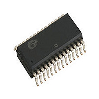
STK10C48-S25I Cypress Semiconductor Corp, STK10C48-S25I Datasheet - Page 8

STK10C48-S25I
Manufacturer Part Number
STK10C48-S25I
Description
Manufacturer
Cypress Semiconductor Corp
Type
NVSRAMr
Datasheet
1.STK10C48-S25I.pdf
(12 pages)
Specifications of STK10C48-S25I
Word Size
8b
Organization
2Kx8
Density
16Kb
Interface Type
Parallel
Access Time (max)
25ns
Operating Supply Voltage (typ)
5V
Package Type
SOIC
Operating Temperature Classification
Industrial
Operating Supply Voltage (max)
5.5V
Operating Supply Voltage (min)
4.5V
Operating Temp Range
-40C to 85C
Pin Count
28
Mounting
Surface Mount
Supply Current
90mA
Lead Free Status / Rohs Status
Not Compliant
March 2006
STK10C48
The STK10C48 has two modes of operation:
mode and nonvolatile mode, determined by the
state of the NE pin. When in
ory operates as a standard fast static
nonvolatile mode, data is transferred in parallel from
SRAM
Elements to
NOISE CONSIDERATIONS
Note that the STK10C48 is a high-speed memory
and so must have a high-frequency bypass capaci-
tor of approximately 0.1μF connected between V
and V
possible. As with all high-speed
careful routing of power, ground and signals will help
prevent noise problems.
SRAM READ
The STK10C48 performs a
and G are low and NE and W are high. The address
specified on pins A
data bytes will be accessed. When the
ated by an address transition, the outputs will be
valid after a delay of t
READ
at t
The data outputs will repeatedly respond to address
changes within the t
for transitions on any control input pins, and will
remain valid until another address change or until E
or G is brought high or W or NE is brought low.
SRAM WRITE
A
low and NE is high. The address inputs must be sta-
ble prior to entering the
remain stable until either E or W goes high at the
end of the cycle. The data on pins DQ
ten into the memory if it is valid t
of a W controlled
E controlled
It is recommended that G be kept high during the
entire
the common I/O lines. If G is left low, internal circuitry
will turn off the output buffers t
WRITE
ELQV
SS
is initiated by E or G, the outputs will be valid
WRITE
to Nonvolatile Elements or from Nonvolatile
or at t
, using leads and traces that are as short as
cycle is performed whenever E and W are
SRAM
WRITE
GLQV
cycle to avoid data bus contention on
, whichever is later (
WRITE
.
0-10
.
AVQV
determines which of the 2,048
AVQV
access time without the need
or t
WRITE
READ
DVEH
(
READ
SRAM
WLQZ
before the end of an
DVWH
CMOS
cycle whenever E
after W goes low.
mode, the mem-
cycle #1). If the
cycle and must
READ
DEVICE OPERATION
before the end
RAM
0-7
READ
ICs, normal
will be writ-
. While in
cycle #2).
is initi-
SRAM
CC
8
NONVOLATILE STORE
A
low and G is high. While any sequence that
achieves this state will initiate a
ation (
#2) are practical without risking an unintentional
SRAM WRITE
STORE
and the
nonvolatile elements. Once a
ated, further input and output are disabled and the
DQ
If E and G are low and W and NE are high at the end
of the cycle, a
puts will go active, signaling the end of the
NONVOLATILE RECALL
A
low and W is high. Like the
initiated when the last of the four clock signals goes
to the
cycle will take t
inputs are ignored. When the
any
effect.
Internally,
SRAM
information is transferred into the
RECALL
nonvolatile cells. The nonvolatile data can be
recalled an unlimited number of times.
As with the
any one control pin to cause a
inadvertent multi-triggering. On power up, once V
exceeds 4.25V, a
ated. Due to this automatic
cannot commence until t
4.25V.
POWER-UP RECALL
During power up, or after any low-power condition
(V
latched. When V
RECALL
take t
STORE
RECALL
CC
0-7
READ
Document Control # ML0002 rev 0.2
< 3.0V), an internal
RESTORE
pins are tri-stated until the cycle is complete.
STORE
data is cleared, and second, the nonvolatile
RECALL
cycle, previous nonvolatile data is erased
cycle will automatically be initiated and will
SRAM
operation in no way alters the data in the
cycle is performed when NE, E and W and
RECALL
cycle is performed when E, G and NE are
or
STORE
to complete.
that would disturb
WRITE
cycle #1) and E initiation (
READ
contents are then programmed into
state. Once initiated, the
NLQX
CC
RECALL
is a two-step procedure. First, the
cycle, a transition must occur on
state on the input pins will take
once again exceeds 4.25V, a
to complete, during which all
will be performed and the out-
RESTORE
cycle is automatically initi-
RECALL
RECALL
STORE
STORE
SRAM
STORE
RECALL
RECALL
after V
,
SRAM
cycle,
SRAM
request will be
data. During a
, only W initi-
cycle is initi-
STORE
, preventing
CC
completes,
RECALL
cells. The
operation
STORE
exceeds
RECALL
cycle
.
CC
is


