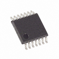
MAX3346EEUD+ Maxim Integrated Products, MAX3346EEUD+ Datasheet - Page 9

MAX3346EEUD+
Manufacturer Part Number
MAX3346EEUD+
Description
IC USB TXRX ESD PROTECT 14TSSOP
Manufacturer
Maxim Integrated Products
Type
Transceiverr
Datasheet
1.MAX3346EEBET.pdf
(17 pages)
Specifications of MAX3346EEUD+
Number Of Drivers/receivers
1/1
Protocol
USB 2.0
Voltage - Supply
4 V ~ 5.5 V
Mounting Type
Surface Mount
Package / Case
14-TSSOP
Lead Free Status / RoHS Status
Lead free / RoHS Compliant
SUSP, or suspend, is a control input. When SUSP is
forced high the MAX3346E enters a low-power state. In
this state, the quiescent supply current into V
than 40µA. In this mode, RCV is forced low, and D+ and
D- are high-impedance inputs (Table 3d).
In suspend mode, data can only be transmitted with
full-speed slope control.
SPEED is a control input that selects between low-speed
(1.5Mbps) and full-speed (12Mbps) USB transmission.
Internally, it selects whether the 1.5kΩ pullup resistor is
connected to D+ (full-speed) or D- (low-speed)
(Functional Diagram). Force SPEED high to select full
speed, or force SPEED low to select low speed.
VTRM is the 3.3V output of the internal linear voltage
regulator. The regulator is used to power the internal
portions of the USB side of the MAX3346E. The VTRM
Figure 1a. Enable and Disable Timing, Receiver
Figure 1b. Enable and Disable Timing, Transmitter
D+/D-
OE
VP/VM
V
0V
L
OE
0V
V
L
_______________________________________________________________________________________
t
t
PZD
PVZ
±15kV ESD-Protected USB Transceiver
V
L
/2
V
L
/2
V
V
OH
OL
- 0.3V
+ 0.3V
V
V
OHD
OLD
CC
t
PDZ
SPEED
+ 0.3V
- 0.3V
VTRM
SUSP
is less
t
PZV
regulator’s supply input is V
greater) ceramic or plastic capacitor from VTRM to
GND, as close to VTRM as possible. Do not use VTRM
to provide power to external circuitry.
D+ and D- are the transceiver I/O connections, and are
ESD protected to ±15kV using the Human Body Model,
making the MAX3346E ideal for applications where a
robust transmitter is required.
Bypass V
1µF capacitor as close as possible to the MAX3346E.
Figure 2. Mode 0 Timing
Figure 3. Mode 1 Timing
VTRM
VPO
0V
0V
V
V
0V
L
VTRM
V
L
0V
L
0V
CC
to GND with a 1µF capacitor. Place the
V
L
/2
t
PHLO
t
t
PHL1
PLH1
V
V
Timing Diagrams
L
/2
L
/2
CC
. Connect a 1.0µF (or
V
in UCSP
L
/2
t
PLHO
D+ and D-
t
t
PLH1
PHL1
VP
VM
D+
D-
V
CC
D+
D-
9


