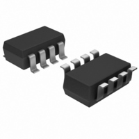
MAX9171EKA+T Maxim Integrated Products, MAX9171EKA+T Datasheet - Page 2

MAX9171EKA+T
Manufacturer Part Number
MAX9171EKA+T
Description
IC RECEIVER LVDS LINE SOT23-8
Manufacturer
Maxim Integrated Products
Type
Receiverr
Datasheet
1.MAX9171EKAT.pdf
(12 pages)
Specifications of MAX9171EKA+T
Number Of Drivers/receivers
0/1
Protocol
LVDS
Voltage - Supply
3 V ~ 3.6 V
Mounting Type
Surface Mount
Package / Case
SOT-23-8
Lead Free Status / RoHS Status
Lead free / RoHS Compliant
ABSOLUTE MAXIMUM RATINGS
V
IN_+, IN_- to GND .................................................-0.3V to +4.0V
OUT_ to GND ............................................-0.3V to (V
Continuous Power Dissipation (T
Single/Dual LVDS Line Receivers with
“In-Path” Fail-Safe
Stresses beyond those listed under “Absolute Maximum Ratings” may cause permanent damage to the device. These are stress ratings only, and functional
operation of the device at these or any other conditions beyond those indicated in the operational sections of the specifications is not implied. Exposure to
absolute maximum rating conditions for extended periods may affect device reliability.
ELECTRICAL CHARACTERISTICS
(V
|V
T
2
LVDS INPUTS (IN_+, IN_-)
Differential Input High Threshold
Differential Input Low Threshold
Input Current (Noninverting Input)
Power-Off Input Current
(Noninverting Input)
Input Current (Inverting Input)
Power-Off Input Current
(Inverting Input)
LVCMOS/LVTTL OUTPUTS (OUT_)
Output High Voltage
Output Low Voltage
Output Short-Circuit Current
POWER SUPPLY
Supply Current
CC
A
ID
CC
8-Pin SOT23 (derate 8.9mW/°C above +70°C) ...........714mW
8-Pin SO (derate 5.9mW/°C above +70°C) .................471mW
8-Pin TDFN (derate 24.4mW/°C above +70°C) ........1951mW
= +25°C.) (Notes 1, 2)
/2| to (V
_______________________________________________________________________________________
to GND ...........................................................-0.3V to +4.0V
= 3.0V to 3.6V, differential input voltage |V
PARAMETER
CC
- |V
ID
/2|), T
A
= -40°C to +85°C, unless otherwise noted. Typical values are at V
A
= +70°C)
SYMBOL
I
I
IN+OFF
IN-OFF
V
V
I
V
V
I
I
I
IN+
CC
IN-
OS
OH
TH
OL
TL
ID
Figure 1
Figure 1
Figure 1
V
or open (Figure 1)
Figure 1
V
or open (Figure 1)
I
I
V
Inputs open
| = 0.1V to 1.2V, receiver input voltage = 0 to V
OH
OL
IN+
IN+
OUT_
CC
= 4.0mA, V
= -4.0mA
= 0 to 3.6V, V
= 0 to 3.6V, V
+ 0.3V)
= 0 (Note 3)
ID
CONDITIONS
Open, undriven short, or
undriven parallel termination
V
MAX9171
MAX9172
ID
= -100mV
IN-
IN-
= 0V
Operating Temperature Range ..........................-40°C to +85°C
Junction Temperature .....................................................+150°C
Storage Temperature Range ............................-65°C to +150°C
ESD Protection
Lead Temperature (soldering, 10s) ................................+300°C
Human Body Model (IN_+, IN_-) ...................................±13kV
= 0 to 3.6V, V
= 0 to 3.6V, V
CC
CC
= 0
= 0
CC
-100
+0.5
MIN
-0.5
-0.5
-0.5
-45
2.7
2.7
CC
= 3.3V, |V
, common-mode voltage V
+4.4
TYP
-2.1
-40
-40
-77
3.2
3.2
0.1
3.6
7.0
0
0
ID
| = 0.2V, V
+10.0
MAX
+0.5
+0.5
-120
-5.0
0.4
0
6
9
CM
UNITS
= 1.2V,
mV
mV
mA
mA
µA
µA
µA
µA
V
V
CM
=


