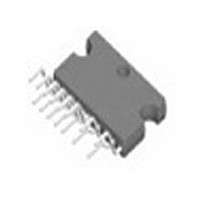
LME49830TB National Semiconductor, LME49830TB Datasheet - Page 5

LME49830TB
Manufacturer Part Number
LME49830TB
Description
Manufacturer
National Semiconductor
Datasheet
1.LME49830TB.pdf
(20 pages)
Specifications of LME49830TB
Operational Class
Class-AB
Audio Amplifier Output Configuration
1-Channel Mono
Audio Amplifier Function
Speaker
Input Offset Voltage
4.2@±100VmV
Total Harmonic Distortion
0.0006@8Ohm%
Single Supply Voltage (typ)
Not RequiredV
Dual Supply Voltage (typ)
±24/±28V
Power Supply Requirement
Dual
Power Dissipation
5.4W
Rail/rail I/o Type
No
Power Supply Rejection Ratio
105dB
Single Supply Voltage (min)
Not RequiredV
Single Supply Voltage (max)
Not RequiredV
Dual Supply Voltage (min)
±20V
Dual Supply Voltage (max)
±100V
Operating Temp Range
-40C to 85C
Operating Temperature Classification
Industrial
Mounting
Through Hole
Pin Count
15 +Tab
Package Type
TO-247
Lead Free Status / Rohs Status
Supplier Unconfirmed
Available stocks
Company
Part Number
Manufacturer
Quantity
Price
Company:
Part Number:
LME49830TB/NOPB
Manufacturer:
AD
Quantity:
101
Company:
Part Number:
LME49830TB/NOPB
Manufacturer:
TI
Quantity:
201
I
I
THD+N
V
A
A
V
V
I
I
SR
V
I
PSRR
PSRR
I
CC
EE
OUT
MUTE
B
AB
BIAS
V(CL)
V(OL)
OM
NOISE
OS
Absolute Maximum Ratings
If Military/Aerospace specified devices are required,
please contact the National Semiconductor Sales Office/
Distributors for availability and specifications.
Electrical Characteristics V
The following specifications apply for I
Supply Voltage |V
Differential Input Voltage
Common Mode Input Range
Power Dissipation (Note 3)
ESD Rating (Note 4)
ESD Rating (Note 5)
Junction Temperature (T
Soldering Information
Symbol
AC
DC
Total Positive Quiescent Power
Supply Current
Total Negative Quiescent Power
Supply Current
Total Harmonic Distortion +
Noise
Bias Voltage
Closed Loop Voltage Gain
Open Loop Gain
Output Voltage Swing
Output Noise
Maximum Output Current
Current into Mute Pin
Slew Rate
Input Offset Voltage
Input Bias Current
Power Supply Rejection Ratio
(AC)
Power Supply Rejection Ratio
(DC)
Bias Control Current
+
| + |V
-
|
JMAX
Parameter
)
MUTE
0.4 V
= 150μA unless otherwise specified. Limits apply for T
CC
EE
(Notes 1, 2)
V
V
No load, f = 1kHz, A
V
f = DC
V
THD = 0.05%, f = 20Hz to 20kHz
R
30kHz BW
A-weighted
Current from Output pins
To put part in “play” mode
V
f = 10kHz square wave, C
V
V
V
R
Input Referred, A
R
A
Shorted output, shorted bias control
to 0.4 V
IN
IN
OUT
IN
IN
CM
CM
CM
V
S
S
S
= +100V, V
= 30dB
= 10kΩ, A
= 1kΩ, f = 100Hz,V
= 1kΩ, Input Referred,
= 1mV
= 0V, V
= 0V, V
= 1.2V
150°C
= 0V, I
= 0V, I
= 0V, I
2.0kV
+/-6V
200V
5.4W
200V
= 30V
CC
RMS
P-P
O
O
O
O
O
RMS
= 0V, I
= 0V, I
, A
= 0mA, I
= 0mA, I
= 0mA
V
, f = 1kHz, C
5
, 30kHz BW
= 30dB,
Conditions
V
V
= 30dB,
= 30dB
Operating Ratings
EE
O
O
Storage Temperature
Thermal Resistance
θ
θ
Temperature Range
Supply Voltage
V
= 0A
= 0A
MUTE
MUTE
= 30dB
TB Package (10 seconds)
T
RIPPLE
JA
JC
MIN
= –100V
LOAD
C
= 150μA
= 0μA
≤
= 10pF
= 1V
T
A
= 2,000pF
≤
RMS
T
MAX
,
(Notes 1, 2)
(Note 6)
Typical
0.0006
±0.9
±0.4
–21
112
104
105
19
16
88
68
44
28
56
39
95
2
A
LME49830
= 25°C.
(Notes 1, 2)
±20V
(Note 7)
Limit
±4.2
−40°C
205
130
250
1.6
2.7
24
15
26
82
47
±3
94
≤
V
-40°C to +150°C
SUPPLY
≤
T
www.national.com
A
mA (max)
mV (max)
mV (max)
mA (max)
≤
≤
μV (max)
mA (min)
nA (max)
mA (min)
dB (min)
dB (min)
μA (min)
dB (min)
(Limits)
73°C/W
V (min)
±100V
Units
4°C/W
260°C
+85°C
V
V/μs
mA
μV
dB
RMS
%


