NBVSPA015LNHTAG ON Semiconductor, NBVSPA015LNHTAG Datasheet

IC VCXO LVDS 200MHZ 6CLCC

NBVSPA015LNHTAG

Manufacturer Part Number
NBVSPA015LNHTAG
Description
IC VCXO LVDS 200MHZ 6CLCC
Manufacturer
ON Semiconductor
Series
PureEdge™r
Type
Voltage Controlled Crystal Oscillator (VCXO)r
Datasheet

Specifications of NBVSPA015LNHTAG

Count
-
Frequency
200MHz
Voltage - Supply
2.97 V ~ 3.63 V
Current - Supply
75mA
Operating Temperature
-40°C ~ 85°C
Package / Case
*
Mounting Type
*
Frequency Stability
50 PPM
Supply Voltage
3.3 Volts
Termination Style
SMD/SMT
Dimensions
3.2 mm W x 5 mm L x 1.35 mm H
Minimum Operating Temperature
- 40 C
Maximum Operating Temperature
+ 85 C
Product
VCXO
Lead Free Status / Rohs Status
Supplier Unconfirmed

Available stocks

Company
Part Number
Manufacturer
Quantity
Price
Part Number:
NBVSPA015LNHTAG
Manufacturer:
ON Semiconductor
Quantity:
70
NBVSPA015 Series
3.3 V, LVDS
Voltage-Controlled Clock
Oscillator (VCXO)
PureEdget Product Series
devices are designed to meet today’s requirements for 3.3 V LVDS
clock generation applications. These devices use a high Q
fundamental mode crystal and Phase Locked Loop (PLL) multiplier to
provide a wide range of frequencies from 60 MHz to 700 MHz
(factory configurable per user specifications) with a pullable range of
±100 ppm and a frequency stability of ±50 ppm. The silicon−based
PureEdge t products design provides users with exceptional
frequency stability and reliability. They produce an ultra low jitter and
phase noise LVDS differential output.
Semiconductor’s PureEdget clock family that provides accurate and
precision clock generation solutions.
smaller 3.2 x 5.0 x 1.2 mm SMD (CLCC) package on 16 mm tape and
reel in quantities of 1,000.
Features
Applications
© Semiconductor Components Industries, LLC, 2010
December, 2010 − Rev. 1
The NBVSPXXXX voltage−controlled crystal oscillator (VCXO)
The NBVSPXXXX series devices are a member of ON
Available in the industry standard 5.0 x 7.0 x 1.8 mm and in a new
Standard Frequencies in the Ordering Information Table on page 6)
1.8 mm and 3.2 x 5.0 x 1.2 mm
LVDS Differential Output
Uses High Q Fundamental Mode Crystal
Ultra Low Jitter and Phase Noise − 0.5 ps (12 kHz − 20 MHz)
Factory Configurable Frequencies from 60 MHz to 700 MHz (see
Pullable Range Minimum of ±100 ppm
Frequency Stability of ±50 ppm
Control Voltage with Positive Slope
Voltage Control Linearity of ±10%
Hermetically Sealed Ceramic SMD Packages of size 5.0 x 7.0 x
Operating Range: 3.3 V ±10%
These Devices are Pb−Free and are RoHS Compliant
Networking
SONET
10 Gigabit Ethernet
Networking Base Stations
Broadcasting
1
See detailed ordering and shipping information in the package
dimensions section on page 6 of this data sheet.
NBVSPXXXX = NBVSPXXXX (±50 ppm)
XXX.XXXX
A
WL
YY
WW
G
CASE 848AB
CASE 848AC
6 PIN CLCC
6 PIN CLCC
LN SUFFIX
LU SUFFIX
ORDERING INFORMATION
http://onsemi.com
= Output Frequency (MHz)
= Assembly Location
= Wafer Lot
= Year
= Work Week
= Pb−Free Package
MARKING DIAGRAMS
Publication Order Number:
NBVSPXXXX
AWLYYWWG
NBVSPXXXX
AWLYYWWG
XXX.XXXX
XXX.XXXX
NBVSPA015/D

Related parts for NBVSPA015LNHTAG

NBVSPA015LNHTAG Summary of contents

Page 1

NBVSPA015 Series 3.3 V, LVDS Voltage-Controlled Clock Oscillator (VCXO) PureEdget Product Series The NBVSPXXXX voltage−controlled crystal oscillator (VCXO) devices are designed to meet today’s requirements for 3.3 V LVDS clock generation applications. These devices use a high Q fundamental mode ...

Page 2

V Crystal 20−30 MHz Table 1. PIN DESCRIPTION Pin No. Symbol I (Note 1) Analog Input LVTTL/LVCMOS Control Input 3 GND Power Supply 4 CLK LVDS Output 5 CLK LVDS Output 6 V Power Supply ...

Page 3

Table 4. MAXIMUM RATINGS Symbol Parameter V Positive Power Supply DD V Control Input (V and OE Output Short Circuit Current OSC CLK or CLK to GND T Operating Temperature Range A T Storage Temperature Range stg ...

Page 4

Table 6. AC CHARACTERISTICS (V Symbol Characteristic f Output Clock Frequency CLKOUT Df Frequency Stability – NBVSPAXXX t (f) RMS Phase Jitter jit t Cycle to Cycle, RMS jitter Cycle to Cycle, Peak−to−Peak Period, RMS Period, Peak−to−Peak t Output Enable/Disable ...

Page 5

Table 8. RELIABILITY COMPLIANCE Parameter Á Á Á Á Á Á Á Á Á Á Á Shock Á Á Á Á Á Á Á Á Á Á Á Á Á Á Á Á Á Á Á Á Á Á Solderability ...

Page 6

Table 9. ORDERING INFORMATION Device Output Frequency (MHz) NBVSPA017LN1TAG NBVSPA018LN1TAG NBVSPA024LN1TAG NBVSPA015LN1TAG NBVSPA027LN1TAG NBVSPA019LN1TAG NBVSPA042LN1TAG NBVSPA017LU1TAG* NBVSPA018LU1TAG* NBVSPA024LU1TAG* NBVSPA015LU1TAG* NBVSPA027LU1TAG* NBVSPA019LU1TAG* NBVSPA042LU1TAG* †For information on tape and reel specifications, including part orientation and tape sizes, please refer to our tape ...

Page 7

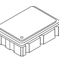
... BOTTOM VIEW SOLDERING FOOTPRINT* PACKAGE OUTLINE *For additional information on our Pb−Free strategy and soldering details, please download the ON Semiconductor Soldering and Mounting Techniques Reference Manual, SOLDERRM/D. CASE 848AC−01 ISSUE O NOTES: 1. DIMENSIONING AND TOLERANCING PER B ASME Y14.5M, 1994. 2. CONTROLLING DIMENSION: MILLIMETERS. ...

Page 8

... L 6X 2.54 PITCH *For additional information on our Pb−Free strategy and soldering details, please download the ON Semiconductor Soldering and Mounting Techniques Reference Manual, SOLDERRM/D. N. American Technical Support: 800−282−9855 Toll Free USA/Canada Europe, Middle East and Africa Technical Support: Phone: 421 33 790 2910 Japan Customer Focus Center Phone: 81− ...

Related keywords