DS92CK16TMTCX/NOPB National Semiconductor, DS92CK16TMTCX/NOPB Datasheet - Page 2
DS92CK16TMTCX/NOPB
Manufacturer Part Number
DS92CK16TMTCX/NOPB
Description
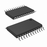
IC TRANSCEIVER 3V BLVDS 24-TSSOP
Manufacturer
National Semiconductor
Type
Transceiverr
Datasheet
1.DS92CK16TMTCNOPB.pdf
(12 pages)
Specifications of DS92CK16TMTCX/NOPB
Number Of Drivers/receivers
1/1
Protocol
LVDS
Voltage - Supply
3 V ~ 3.6 V
Mounting Type
Surface Mount
Package / Case
24-TSSOP
Number Of Transmitters
1
Power Supply Requirement
Single
Package Type
TSSOP
Operating Temperature Classification
Industrial
Mounting
Surface Mount
Operating Temperature (max)
85C
Operating Temperature (min)
-40C
Supply Current
25mA
Dual Supply Voltage (typ)
Not RequiredV
Dual Supply Voltage (max)
Not RequiredV
Dual Supply Voltage (min)
Not RequiredV
Lead Free Status / RoHS Status
Lead free / RoHS Compliant
Other names
DS92CK16TMTCX


www.national.com
CLKI/O+
CLKI/O−
OE
DE
CLK
CrdCLK
V
GND
V
GNDA
NC
Connection Diagram
TSSOP Package Pin Descriptions
CC
CCA
Pin Name
OUT
IN
13, 15, 17, 19, 21, 23
1, 12, 14, 18, 22
16, 20, 24
Pin #
3, 10
5, 8
11
6
7
2
9
4
Ground
Ground
Power
Power
Type
I/O
I/O
See NS Package Number MTC24
O
Order Number DS92CK16TMTC
I
I
I
True (Positive) side of the differential clock input.
Complementary (Negative) side of the differential clock input.
OE; this pin is active Low. When High, this pin forces all CLK
High. When Low, CLK
CrdCLK
at the DE pin. This pin has a weak pullup device to V
floating, then all CLK
DE; this pin is active LOW. When Low, this pin enables the
CardCLK
the Driver is TRI-STATE
the state of the CLK
V
6 Buffered clock (CMOS) outputs.
Input clock from Card (CMOS level or TTL level).
V
use separate power supplies). No special power sequencing required.
Either V
power supplies.
GND
Analog V
separate power supplies). No special power sequencing required.
Either V
power supplies.
Analog Ground (Internally separate from Ground must be connected
externally).
No Connects
CC
CC
. If DE is floating, then CLKI/O pins are TRI-STATE.
; Analog V
2
IN
CCA
CCA
IN
CCA
or the VID at the CLK/I/O pins with respect to the logic level
signal to the CLKI/O pins and CLK
or V
or V
(Internally separate from V
CCA
CC
CC
(Internally separate from V
can be applied first, or simultaneously apply both
can be applied first, or simultaneously apply both
OUT
10108202
OUT
OUT
®
pins. This pin has a weak pullup device to
pins will be High.
, the CLKI/O pins are inputs and determine
pins logic state is determined by either the
Description
CC
, connect externally or use
CC
OUT
, connect externally or
pins. When High,
CC
. If OE is
OUT
pins
Related parts for DS92CK16TMTCX/NOPB
Image
Part Number
Description
Manufacturer
Datasheet
Request
R

Part Number:
Description:
3V BLVDS 1 to 6 Clock Buffer/Bus Transceiver
Manufacturer:
National Semiconductor
Datasheet:
Part Number:
Description:
National Semiconductor [8-Bit D/A Converter]
Manufacturer:
National Semiconductor
Datasheet:
Part Number:
Description:
National Semiconductor [Media Coprocessor]
Manufacturer:
National Semiconductor
Datasheet:
Part Number:
Description:
Digitally Controlled Tone and Volume Circuit with Stereo Audio Power Amplifier, Microphone Preamp Stage and National 3D Sound
Manufacturer:
National Semiconductor
Datasheet:
Part Number:
Description:
Digitally Controlled Tone and Volume Circuit with Stereo Audio Power Amplifier, Microphone Preamp Stage and National 3D Sound
Manufacturer:
National Semiconductor
Datasheet:
Part Number:
Description:
AC97 Rev 2 Codec with Sample Rate Conversion and National 3D Sound
Manufacturer:
National Semiconductor
Part Number:
Description:
Manufacturer:
National Semiconductor
Datasheet:
Part Number:
Description:
Manufacturer:
National Semiconductor
Datasheet:
Part Number:
Description:
General Purpose, Low Voltage, Low Power, Rail-to-Rail Output Operational Amplifiers
Manufacturer:
National Semiconductor
Datasheet:
Part Number:
Description:
8-bit 20 MSPS flash A/D converter.
Manufacturer:
National Semiconductor
Datasheet:
Part Number:
Description:
Low Noise Quad Operational Amplifier
Manufacturer:
National Semiconductor
Datasheet:
Part Number:
Description:
Quad Differential Line Receivers
Manufacturer:
National Semiconductor
Datasheet:
Part Number:
Description:
Quad High Speed Trapezoidal? Bus Transceiver
Manufacturer:
National Semiconductor
Datasheet:
Part Number:
Description:
Dual Line Receiver
Manufacturer:
National Semiconductor
Datasheet: