DS26LV31TM/NOPB National Semiconductor, DS26LV31TM/NOPB Datasheet
DS26LV31TM/NOPB
Specifications of DS26LV31TM/NOPB
*DS26LV31TM/NOPB
DS26LV31TM
Available stocks


Related parts for DS26LV31TM/NOPB

DS26LV31TM/NOPB Summary of contents
Page 1
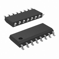
... Top View Order Number DS26LV31TM or DS26LV31W See NS Package Number M16A or W16A TRI-STATE ® registered trademark of National Semiconductor Corporation. © 2004 National Semiconductor Corporation n Interoperable with existing 5V RS-422 networks n Industrial and Military temperature range n Guaranteed V n Balanced output crossover for low EMI (typical within 50% voltage level) n Low power design (330 µ ...
Page 2
... Absolute Maximum Ratings If Military/Aerospace specified devices are required, please contact the National Semiconductor Sales Office/ Distributors for availability and specifications. Supply Voltage ( Enable Input Voltage (EN, EN*) Driver Input Voltage (DI) Clamp Diode Current DC Output Current, per pin Driver Output Voltage (Power Off: DO+, DO−) ...
Page 3
Switching Characteristics - Industrial Over supply voltage and -40˚C to +85˚C operating temperature range, unless otherwise specified Sym Parameter t Differential Propagation Delay PHLD High to Low t Differential Propagation Delay PLHD Low to High t Differential Skew (same SKD ...
Page 4
Parameter Measurement Information FIGURE 2. Differential Driver Propagation Delay and Transition Time Test Circuit FIGURE 3. Differential Driver Propagation Delay and Transition Time Waveforms Note 11: Generator waveform for all tests unless otherwise specified MHz, Duty Cycle ...
Page 5
Parameter Measurement Information the input, then EN* = High If EN* is the input, then EN = Low FIGURE 4. Driver Single-Ended TRI-STATE Test Circuit FIGURE 5. Driver Single-Ended TRI-STATE Waveforms (Continued) 01264205 01264206 5 www.national.com ...
Page 6
Typical Application Information General application guidelines and hints for differential driv- ers and receivers may be found in the following application notes: AN-214, AN-457, AN-805, AN-847, AN-903, AN-912, AN- 916 optional although highly recommended to reduce reflection. T ...
Page 7
Physical Dimensions inches (millimeters) unless otherwise noted 16-Lead Molded Small Outline Package (M) Order Number DS26LV31TM NS Package Number M16A 7 www.national.com ...
Page 8
... BANNED SUBSTANCE COMPLIANCE National Semiconductor certifies that the products and packing materials meet the provisions of the Customer Products Stewardship Specification (CSP-9-111C2) and the Banned Substances and Materials of Interest Specification (CSP-9-111S2) and contain no ‘‘Banned Substances’’ as defined in CSP-9-111S2. ...