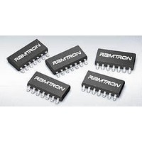
FM3204-G Ramtron, FM3204-G Datasheet - Page 14

FM3204-G
Manufacturer Part Number
FM3204-G
Description
Supervisory Circuits 4K w/Pwr Mon WDT Bat Sw Pwr Fail
Manufacturer
Ramtron
Datasheet
1.FM3264-G.pdf
(21 pages)
Specifications of FM3204-G
Number Of Voltages Monitored
4
Monitored Voltage
2.6 V or 2.9 V or 3.9 V or 4.4 V
Output Type
Active Low or Bidirectional
Manual Reset
Resettable
Watchdog
Watchdog
Battery Backup Switching
Backup
Power-up Reset Delay (typ)
200 ms
Supply Voltage (max)
5.5 V
Supply Voltage (min)
2.7 V
Supply Current (typ)
1500 uA
Maximum Operating Temperature
+ 85 C
Mounting Style
SMD/SMT
Package / Case
SOIC-14
Minimum Operating Temperature
- 40 C
Power Fail Detection
Yes
Lead Free Status / Rohs Status
Lead free / RoHS Compliant
three bytes of a write operation to set the internal
address followed by subsequent read operations.
To perform a selective read, the bus master sends out
the slave address with the LSB set to 0. This specifies
a write operation. According to the write protocol,
the bus master then sends the address bytes that are
loaded into the internal address latch. After the
FM32xx acknowledges the address, the bus master
issues a Start condition. This simultaneously aborts
the write operation and allows the read command to
be issued with the slave address LSB set to a 1. The
operation is now a read from the current address.
Read operations are illustrated below.
Companion Write Operation
All Companion writes operate in a similar manner to
memory writes. The distinction is that a different
device ID is used and only one byte of address is
needed instead of two. Figure 15 illustrates a single
byte write to this device.
Companion Read Operation
As with writes, a read operation begins with the
Slave Address. To perform a register read, the bus
Rev. 3.1
July 2010
By FM32xx
By Master
By FM32xx
By Master
Start
S
Slave Address
Start
Address
S
Figure 12. Current Address Memory Read
Slave Address
Figure 13. Sequential Memory Read
Acknowledge
Address
1
A
Acknowledge
Data Byte
1
A
master supplies a Slave Address with the LSB set to
1. This indicates that a read operation is requested.
After receiving the complete Slave Address, the
FM32xx will begin shifting data out from the current
register address on the next clock. Auto-increment
operates for the special function registers as with the
memory address. A current address read for the
registers look exactly like the memory except that the
device ID is different.
The FM32xx contains two separate address registers,
one for the memory address and the other for the
register address. This allows the contents of one
address register to be modified without affecting the
current address of the other register. For example,
this would allow an interrupted read to the memory
while still providing fast access to a companion
register. A subsequent memory read will then
continue from the memory address where it
previously left off, without requiring the load of a
new memory address. However, a write sequence
always requires an address to be supplied.
Acknowledge
Data Byte
Data
A
Data
Acknowledge
Data Byte
No
1
P
Acknowledge
FM3204/16/64/256
No
1 P
Stop
Page 14 of 21
Stop


