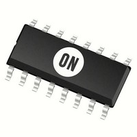
MC44603DW ON Semiconductor, MC44603DW Datasheet - Page 18

MC44603DW
Manufacturer Part Number
MC44603DW
Description
Other Power Management Voltage/Current PWM
Manufacturer
ON Semiconductor
Type
PWM Mode Controllerr
Datasheet
1.MC44603DWR2.pdf
(24 pages)
Specifications of MC44603DW
Input Voltage Range
18 V
Mounting Style
SMD/SMT
Package / Case
SOIC-16 Wide
Lead Free Status / Rohs Status
Lead free / RoHS Compliant
standby losses mainly consist of the energy waste due to:
Losses can be considered constant. This waste of energy
decreases when the standby losses are reduced.
increased (each switching requires some energy to turn on
the power switch).
frequency.
decreasing the switching frequency as much as possible.
frequency lower than the normal working one.
•
transformer during the on−time to be transferred to the
output during the off−time, is equal to:
where:
Input power is labelled P
where f
AC Line
In a classical flyback (as depicted in Figure 40), the
− the startup resistor R
− the consumption of the IC and the power
−
− the inrush current limitation resistor R
− the switching losses in the power switch → P
− the snubber and clamping network
P
P
P
P
Consequently, standby losses can be minimized by
The MC44603A was designed to operate at a standby
During a switching period, the energy drawn by the
− L is the transformer primary inductor,
− l
Standby Power Calculations with MC44603A
startup
ICL
control
SW
switch control
pk
R
ICL
only depends on the current drawn from the mains.
is the inductor peak current.
S
and P
Figure 40. Power Losses in a Classical
is the normal working switching frequency.
is nearly constant and is equal to:
increases when the oscillator frequency is
V
in
SN−CLN
P in + 0.5 x L x I pk 2 x f S
+
(V in –V CC ) 2 R startup
MC44603A
Flyback Structure
E + 1
V
R
CC
startup
are proportional to the switching
startup
in
2
:
x L x I pk 2
Clamping
Network
R
Snubber
S
ICL
→ P
→ P
→ P
→ P
+
control
SW
SN−CLN
startup
ICL
http://onsemi.com
18
Also,
where R
current.
the internal current sense comparator input).
a V
the threshold level by connecting a resistor to Pin 12.
noninverting input voltage is typically equal to (3.0 x V
V
[(V
labelled P
And as:
V
x (V
an oscillator discharge current reduction in order to increase
the oscillator period and to diminish the switching
frequency. As it is represented in Figure 41, the (0.8 x I
current source is disconnected and is replaced by a lower
value one (0.25 x I
Where: I
ER
F
CS
R
Thus, the input power is proportional to V
That is why the standby detection is performed by creating
As depicted in Figure 41, the standby comparator
The V
Thus, when the power drawn by the converter decreases,
) while the inverter input value is (V
P Stby
CS
12
13
R P Stby
AmpOut
R P Stby
decreases and when V
threshold. An internal current source (0.4 x I
R P Stby +
0.4 I
S
P thL + 0.5 x L x
F Stby
thL
is the resistor used to measure the power switch
CS
V R P Stby + R P Stby x 0.4 x I ref
)/3] and if the corresponding power threshold is
ref
)/3], the standby mode is activated. This results in
V
:
ref
= V
threshold level is typically equal to
0
V
ref
ref
F Stby
0.6 I
Figure 41. Standby
1
2R
1R
/R
10.6 x R S x R ref
+ R R P Stby x 0.4 x
ref
C
F Stby
Stby
I pk +
).
C. S. Comparator
V ref
CS
0.8 I
V R P Stby
V CS
3.0 R S
becomes lower than [V
ref
R S
1
V
ref
I
Discharge/2
V
ref
0
0.25
I
x
F Stby
R P Stby
2
Current Mirror X2
x f S
R ref
V ref
L x f S
CS
P thL
V
I
2
ref
Discharge
0.2 I
+ V
(V
Discharge
Oscillator
ref
Current
CS
F
ref
).
being
) sets
CS−th
CS
ref
+
)


