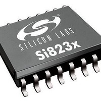
Si8230-A-IS Silicon Laboratories Inc, Si8230-A-IS Datasheet - Page 15

Si8230-A-IS
Manufacturer Part Number
Si8230-A-IS
Description
MOSFET & Power Driver ICs 0.5A HS/LS ISOdriver Dual Input
Manufacturer
Silicon Laboratories Inc
Type
High and Low Sider
Datasheet
1.SI8234BD-C-IS.pdf
(52 pages)
Specifications of Si8230-A-IS
Rise Time
12 ns
Fall Time
12 ns
Propagation Delay Time
50 ns
Supply Voltage (max)
24 V
Supply Voltage (min)
10 V
Supply Current
11 mA
Maximum Operating Temperature
+ 125 C
Mounting Style
SMD/SMT
Package / Case
SOIC-16
Bridge Type
Half Bridge
Minimum Operating Temperature
- 40 C
Number Of Drivers
2
Number Of Outputs
2
Output Current
0.5 A
Lead Free Status / Rohs Status
Lead free / RoHS Compliant
3. Functional Description
The operation of an Si823x channel is analogous to that of an opto coupler and gate driver, except an RF carrier is
modulated instead of light. This simple architecture provides a robust isolated data path and requires no special
considerations or initialization at start-up. A simplified block diagram for a single Si823x channel is shown in
Figure 8.
A channel consists of an RF Transmitter and RF Receiver separated by a semiconductor-based isolation barrier.
Referring to the Transmitter, input A modulates the carrier provided by an RF oscillator using on/off keying. The
Receiver contains a demodulator that decodes the input state according to its RF energy content and applies the
result to output B via the output driver. This RF on/off keying scheme is superior to pulse code schemes as it
provides best-in-class noise immunity, low power consumption, and better immunity to magnetic fields. See
Figure 9 for more details.
A
Transmitter
control
Dead
time
OSCILLATOR
MODULATOR
Figure 8. Simplified Channel Diagram
RF
Figure 9. Modulation Scheme
Semiconductor-
Based Isolation
Barrier
Rev. 1.1
DEMODULATOR
Receiver
Modulation Signal
Output Signal
Input Signal
Driver
Gnd
V
DD
Si823x
0.5 to 4 A
peak
B
15


