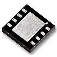
LMH6553SD National Semiconductor, LMH6553SD Datasheet - Page 16

LMH6553SD
Manufacturer Part Number
LMH6553SD
Description
DIFF AMP, 900MHZ, 8LLP, POWERWISE
Manufacturer
National Semiconductor
Datasheet
1.LMH6553SDE.pdf
(24 pages)
Specifications of LMH6553SD
No. Of Amplifiers
1
Gain Db Max
1dB
Bandwidth
900MHz
Slew Rate
2300V/µs
Supply Voltage Range
4.5V To 12V
Supply Current
29.1mA
Amplifier Case Style
LLP
No. Of Pins
8
Rohs Compliant
Yes
www.national.com
Application Information
The LMH6553, a fully differential current feedback amplifier
with integrated output common mode control and output lim-
iting clamp, is designed to provide protection of following input
stages. The common mode feedback circuit sets the output
common mode voltage independent of the input common
mode, as well as forcing the outputs to be equal in magnitude
and opposite in phase, even when only one of the inputs is
driven as in single ended to differential conversion.
The proprietary current feedback architecture of the
LMH6553 offers gain and bandwidth independence even at
high values of gain, simply with the appropriate choice of
R
to R
these resistors greatly affects CMRR, DC offset error, and
output balance. Resistors with 0.1% tolerances are recom-
mended for optimal performance, and the amplifier is inter-
nally compensated to operate with optimum gain flatness with
values of R
selection, PCB layout, and load resistance.
The output common mode voltage is set by the V
a fixed gain of 1 V/V. This pin should be driven by a low
impedance source and should be bypassed to ground with a
0.1 µF ceramic capacitor. Any unwanted signal coupling into
the V
performance of the amplifier. This pin must not be left floating.
The LMH6553 can be operated with either a single 5V supply
or split +5V and −5V supplies. Operation on a single 5V sup-
ply, depending on gain, is limited by the input common mode
range; therefore, AC coupling may be required. For example,
in a DC coupled input application on a single 5V supply, with
a V
0.75V which is outside the minimum 1.5V to 3.5V input com-
mon mode range of the amplifier. The minimum V
application should be greater than 1.5V depending on output
signal swing. Alternatively, AC coupling of the inputs in this
example results in equal input and output common mode volt-
ages, so a 1.5V input common mode would result. Split
supplies allow much less restricted AC and DC coupled op-
eration with optimum distortion performance.
The LMH6553 has a V
maximum amplifier output swing to prevent overdriving of fol-
lowing stages such as sensitive ADC inputs and also provides
fast recovery from transients that would otherwise saturate
the signal path.
RECOMMENDED FEEDBACK RESISTOR
The LMH6553 is available in both an 8-pin LLP and PSOP
package. The recommended feedback resistor, R
LLP package is 275Ω and 325Ω for the PSOP to give a flat
frequency response with minimal peaking.
FULLY DIFFERENTIAL OPERATION
The LMH6553 is ideal for a fully differential configuration. The
circuit shown in Figure 1 is a typical fully differential applica-
tion circuit as might be used to drive an analog to digital
converter (ADC). In this circuit the closed loop gain
A
The series output resistors, R
the amplifier stable when presented with a capacitive load.
Refer to the Driving Capacitive Loads section for details.
F1
V
CM
= V
and R
G2
CM
, so that the gain is set by the ratio R
of 1.5V, the input common voltage at a gain of 1 will be
OUT
pin will be passed along to the outputs, reducing the
F2
/ V
F
. Generally R
between 250Ω and 350Ω depending on package
IN
= R
F
/R
CLAMP
G
, where the feedback is symmetric.
F1
is set equal to R
input which allows control of the
O
, are optional and help keep
F
F2
/R
, and R
G
. Matching of
CM
CM
F
G1
, for the
pin with
for this
equal
16
When driven from a differential source, the LMH6553 pro-
vides low distortion, excellent balance, and common mode
rejection. This is true provided the resistors R
are well matched and strict symmetry is observed in board
layout.
The circuit configuration shown in Figure 2 was used to mea-
sure differential S parameters in a 50Ω environment at a gain
of 1 V/V. Refer to the Differential S-Parameter vs. Frequency
plots in the Typical Performance Characteristics section for
measurement results.
SINGLE-ENDED INPUT TO DIFFERENTIAL OUTPUT
OPERATION
In many applications, it is required to drive a differential input
ADC from a single-ended source. Traditionally, transformers
have been used to provide single to differential conversion,
but these are inherently bandpass by nature and cannot be
used for DC coupled applications. The LMH6553 provides
excellent performance as a single-to-differential converter
down to DC. Figure 3 shows a typical application circuit where
an LMH6553 is used to produce a differential signal from a
single ended source.
FIGURE 2. Differential S-Parameter Test Circuit
FIGURE 1. Typical Application
F
, R
G
30043753
30043770
and R
O


