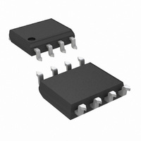
DS90LV028AQMAX/NOPB National Semiconductor, DS90LV028AQMAX/NOPB Datasheet - Page 3

DS90LV028AQMAX/NOPB
Manufacturer Part Number
DS90LV028AQMAX/NOPB
Description
IC LINE RCVR LVDS DUAL 3V 8SOIC
Manufacturer
National Semiconductor
Type
Line Receiverr
Datasheet
1.DS90LV028AQMANOPB.pdf
(10 pages)
Specifications of DS90LV028AQMAX/NOPB
Number Of Drivers/receivers
0/2
Protocol
LVDS
Voltage - Supply
3 V ~ 3.6 V
Mounting Type
Surface Mount
Package / Case
8-SOIC (3.9mm Width)
Lead Free Status / RoHS Status
Lead free / RoHS Compliant
Other names
DS90LV028AQMAX
Note 7: Output short circuit current (I
exceed maximum junction temperature specification.
Note 8: C
Note 9: Generator waveform for all tests unless otherwise specified: f = 1 MHz, Z
Note 10: t
channel.
Note 11: t
the integrated circuit.
Note 12: t
V
Note 13: t
recommended operating temperature and voltage ranges, and across process distribution. t
Note 14: f
cycle, V
Parameter Measurement Information
Typical Application
CC
and within 5°C of each other within the operating temperature range.
OL
L
SKD1
SKD3
SKD2
(max 0.4V), V
SKD4
MAX
includes probe and jig capacitance.
, part to part skew, is the differential channel-to-channel skew of any event between devices. This specification applies to devices at the same
generator input conditions: t
is the magnitude difference in differential propagation delay time between the positive-going-edge and the negative-going-edge of the same
, part to part skew, is the differential channel-to-channel skew of any event between devices. This specification applies to devices over the
is the differential channel-to-channel skew of any event on the same device. This specification applies to devices having multiple receivers within
OH
(min 2.7V), load = 15 pF (stray plus probes).
FIGURE 1. Receiver Propagation Delay and Transition Time Test Circuit
FIGURE 2. Receiver Propagation Delay and Transition Time Waveforms
OS
) is specified as magnitude only, minus sign indicates direction only. Only one output should be shorted at a time, do not
r
= t
f
< 1 ns (0% to 100%), 50% duty cycle, differential (1.05V to 1.35 peak to peak). Output criteria: 60%/40% duty
FIGURE 3. Point-to-Point Application
Balanced System
3
O
= 50Ω, t
r
SKD4
and t
is defined as |Max − Min| differential propagation delay.
f
(0% to 100%)
30064103
30064105
≤
3 ns for R
30064104
IN
.
www.national.com


