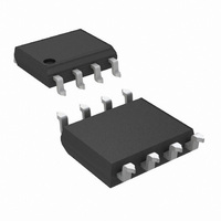
DS92LV010ATMX/NOPB National Semiconductor, DS92LV010ATMX/NOPB Datasheet - Page 8

DS92LV010ATMX/NOPB
Manufacturer Part Number
DS92LV010ATMX/NOPB
Description
IC TRANSCEIVER SINGLE BUS 8-SOIC
Manufacturer
National Semiconductor
Type
Transceiverr
Datasheet
1.DS92LV010ATMNOPB.pdf
(10 pages)
Specifications of DS92LV010ATMX/NOPB
Number Of Drivers/receivers
1/1
Protocol
LVDS
Voltage - Supply
3 V ~ 5.5 V
Mounting Type
Surface Mount
Package / Case
8-SOIC (3.9mm Width)
Lead Free Status / RoHS Status
Lead free / RoHS Compliant
Other names
*DS92LV010ATMX
*DS92LV010ATMX/NOPB
DS92LV010ATMX
*DS92LV010ATMX/NOPB
DS92LV010ATMX
Available stocks
Company
Part Number
Manufacturer
Quantity
Price
Company:
Part Number:
DS92LV010ATMX/NOPB
Manufacturer:
TI
Quantity:
3 400
Part Number:
DS92LV010ATMX/NOPB
Manufacturer:
TI/德州仪器
Quantity:
20 000
www.national.com
Application Information
There are a few common practices which should be implied
when designing PCB for BLVDS signaling. Recommended
practices are:
•
•
•
•
•
Use at least 4 layer PCB board (BLVDS signals, ground,
power and TTL signals).
Keep drivers and receivers as close to the (BLVDS port
side) connector as possible.
Bypass each BLVDS device and also use distributed bulk
capacitance. Surface mount capacitors placed close to
power and ground pins work best. Two or three multi-layer
ceramic (MLC) surface mount capacitors (0.1 µF, and 0.01
µF in parallel should be used between each V
ground. The capacitors should be as close as possible to
the V
Use the termination resistor which best matches the
differential impedance of your transmission line.
Leave unused LVDS receiver inputs open (floating)
LOOP BACK MODE
MODE SELECTED
TRI-STATE MODE
RECEIVER MODE
DRIVER MODE
CC
Pin Name
DO±/RI±
pin.
R
GND
DIN
V
RE
DE
OUT
CC
TABLE 1. Functional Table
Pin #
6, 7
2
3
5
1
4
8
DE
H
H
L
L
Input/Output
TABLE 4. Device Pin Descriptions
CC
RE
I/O
NA
NA
H
H
L
L
O
and
I
I
I
8
TTL Driver Input
LVDS Driver Outputs/LVDS Receiver Inputs
TTL Receiver Output
Receiver Enable TTL Input (Active Low)
Driver Enable TTL Input (Active High)
Ground
Power Supply
L = Low state
H = High state
X = High or Low logic state
Z = High impedance state
L = Low state
H = High state
RE
DE
H
L
L
L
H
H
H
L
INPUTS
2 > & > 0.8
TABLE 2. Transmitter Mode
TABLE 3. Receiver Mode
100 mV > & > −100 mV
Description
DI
H
X
L
INPUTS
H (> +100 mV)
L (< −100 mV)
(RI+)-(RI−)
X
DO+
H
L
X
Z
OUTPUTS
DO−
H
L
X
Z
OUTPUT
H
X
L
Z


