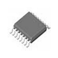
DS90LV049HMTX National Semiconductor, DS90LV049HMTX Datasheet - Page 4

DS90LV049HMTX
Manufacturer Part Number
DS90LV049HMTX
Description
IC LDRVR/RCVR PAIR LVDS 16-TSSOP
Manufacturer
National Semiconductor
Type
Line Transceiverr
Datasheet
1.DS90LV049HMTX.pdf
(10 pages)
Specifications of DS90LV049HMTX
Number Of Drivers/receivers
2/2
Protocol
RS644
Voltage - Supply
3 V ~ 3.6 V
Mounting Type
Surface Mount
Package / Case
16-TSSOP
Number Of Elements
2
Number Of Receivers
2
Number Of Drivers
2
Input Type
CMOS/TTL
Operating Supply Voltage (typ)
3.3V
Differential Input High Threshold Voltage
35mV
Diff. Input Low Threshold Volt
-100mV
Differential Output Voltage
450mV
Transmission Data Rate
400Mbps
Propagation Delay Time
3.5ns
Operating Temp Range
-40C to 125C
Operating Temperature Classification
Automotive
Mounting
Surface Mount
Pin Count
16
Package Type
TSSOP
Lead Free Status / RoHS Status
Contains lead / RoHS non-compliant
Other names
DS90LV049HMTXTR
Available stocks
Company
Part Number
Manufacturer
Quantity
Price
Company:
Part Number:
DS90LV049HMTX/NOPB
Manufacturer:
NS
Quantity:
16 578
www.national.com
Switching Characteristics
Note 8: t
the same device.
Note 9: t
specified differential propagation delays. This specification applies to devices at the same V
Note 10: t
going edge of the same receiver channel.
Note 11: t
Note 12: t
propagation delays. This specification applies to devices at the same V
Note 13: Generator waveform for all tests unless otherwise specified: f = 1 MHz, Z
Note 14: Output short circuit current (I
Note 15: All input voltages are for one channel unless otherwise specified. Other inputs are set to GND.
Note 16: f
switching.
Note 17: f
Parameter Measurement Information
>
2.7 V, V
SKD2
SKD3
SK1
SK2
SK3
MAX
MAX
OL
<
or differential channel-to-channel skew is defined as the magnitude difference in the differential propagation delays between two driver channels on
or differential part-to-part skew is defined as |t
or pulse skew is defined as |t
or channel-to-channel skew is defined as the magnitude difference in the propagation delays between two receiver channels on the same device.
or part-to-part skew is defined as |t
generator input conditions: t
generator input conditions: t
0.25 V, all channels switching.
FIGURE 2. Driver Propagation Delay and Transition Time Test Circuit
OS
) is specified as magnitude only, minus sign indicates direction only.
r
r
= t
PHL
= t
f
<
f
− t
<
1 ns (0% to 100%), 50% duty cycle, 0 V to 3 V. Output Criteria: duty cycle = 45%/55%, V
PLH Max
PLH
1 ns (0% to 100%), 50% duty cycle, V
FIGURE 1. Driver V
|. It is the magnitude difference in the propagation delays between the positive going edge and the negative
(Continued)
− t
PLHD Max
PLH Min
− t
| or |t
DD
PLHD Min
PHL Max
and within 5˚C of each other within the operating temperature range.
OD
| or |t
4
and V
− t
O
PHLD Max
PHL Min
= 50 Ω, t
ID
OS
DD
= 200 mV, V
|. It is the difference between the minimum and maximum specified
and within 5˚C of each other within the operating temperature range.
Test Circuit
− t
r
PHLD Min
≤ 1 ns, and t
CM
|. It is the difference between the minimum and maximum
= 1.2 V . Output Criteria: duty cycle = 45%/55%, V
f
≤ 1 ns.
20161703
OD
>
250 mV, all channels
20161704
OH


