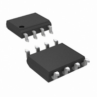
DS89C21TMX/NOPB National Semiconductor, DS89C21TMX/NOPB Datasheet - Page 2

DS89C21TMX/NOPB
Manufacturer Part Number
DS89C21TMX/NOPB
Description
IC LINE DVR/RVR DIFF PAIR 8-SOIC
Manufacturer
National Semiconductor
Type
Transceiverr
Datasheet
1.DS89C21TMNOPB.pdf
(6 pages)
Specifications of DS89C21TMX/NOPB
Number Of Drivers/receivers
1/1
Protocol
RS422
Voltage - Supply
4.5 V ~ 5.5 V
Mounting Type
Surface Mount
Package / Case
8-SOIC (3.9mm Width)
Data Rate
20Mbps
Number Of Receivers
1
Number Of Transmitters
1
Number Of Transceivers
1
Data Transmission Topology
Multidrop
Receiver Signal Type
Differential
Transmitter Signal Type
Differential
Single Supply Voltage (typ)
5V
Single Supply Voltage (min)
4.5V
Single Supply Voltage (max)
5.5V
Dual Supply Voltage (typ)
Not RequiredV
Dual Supply Voltage (min)
Not RequiredV
Dual Supply Voltage (max)
Not RequiredV
Supply Current
12mA
Power Supply Requirement
Single
Operating Temp Range
-40C to 85C
Operating Temperature Classification
Industrial
Mounting
Surface Mount
Pin Count
8
Package Type
SOIC N
Lead Free Status / RoHS Status
Lead free / RoHS Compliant
Other names
*DS89C21TMX
*DS89C21TMX/NOPB
DS89C21TMX
*DS89C21TMX/NOPB
DS89C21TMX
Available stocks
Company
Part Number
Manufacturer
Quantity
Price
Company:
Part Number:
DS89C21TMX/NOPB
Manufacturer:
DM
Quantity:
6 221
www.national.com
DRIVER CHARACTERISTICS
V
V
I
V
V
V
∆V
V
V
V
∆V
I
I
RECEIVER CHARACTERISTICS
V
V
R
I
IH
OSD
OFF
IN
Symbol
IH
IL
CL
OD1
OD2
OD3
OD4
OC
TL
HYS
IN
Absolute Maximum Ratings
If Military/Aerospace specified devices are required,
please contact the National Semiconductor Sales Office/
Distributors for availability and specifications.
Electrical Characteristics
Over recommended supply voltage and operating temperature ranges, unless otherwise specified.
, I
OD2
OC
, V
IL
TH
Supply Voltage (V
Driver Input Voltage (DI)
Driver Output Voltage (DO,
DO
Receiver Input Voltage — V
CM
Differential Receiver Input
Receiver Output Voltage
(RO)
Receiver Output Current
(RO)
Storage Temperature
Range
(RI, RI
Voltage — V
*
)
Input Voltage HIGH
Input Voltage LOW
Input Current
Input Clamp Voltage
Unloaded Output Voltage
Differential Output Voltage
Change in Magnitude of V
for Complementary Output States
Differential Output Voltage
Differential Output Voltage
Common Mode Voltage
Change in Magnitude of V
for Complementary Output States
Output Short Circuit Current
Output Leakage Current
Differential Thresholds
Hysteresis
Input Impedance
Input Current
*
)
DIFF
Parameter
CC
(RI, RI
)
*
)
−1.5V to V
−0.5V to V
OD2
OC
−0.5V to +7V
(Notes 2, 3)
CC
CC
±
(Note 1)
V
I
No Load
R
R
R
R
V
V
V
V
V
Other Input = 0V,
V
V
+ 1.5V
25 mA
IN
+0.5V
CC
CC
CC
±
±
IN
L
L
L
OUT
IN
CM
IN
L
14V
14V
= −18 mA
= 100Ω
= 150Ω
= 3.9 kΩ
= 100Ω
7V
= V
= +7V, 0V, −7V
= 0V
= −7V, +7V, Other = 0V
= 5.5V and
= 0V
= 0V
= 0V
CC
, GND, 2.0V, 0.8V
2
Conditions
Recommended Operating
Conditions
Supply Voltage (V
Operating Temperature (T
Input Rise or Fall Time (DI)
V
V
V
V
V
V
V
OUT
OUT
IN
IN
IN
IN
IN
Lead Temperature (T
Maximum Junction
Temperature
Maximum Package Power Dissipation
Derate M Package
= +10V
= +3.0V
= +0.5V
= −3V
= −10V
(T
(Soldering 4 sec.)
M Package
= +6V
= −0.25V
STG
)
CC
)
L
DO,
Pin
DO*
RI,
)
A
DI
RI*
)
GND
−200
Min
−30
2.0
2.0
2.1
5.0
20
0
0
4.50
Min
−40
5.7 mW/˚C above
−65˚C to +150˚C
−0.08
+0.22
−0.04
−0.41
−1.25
−115
0.05
0.03
+1.0
Typ
±
4.2
3.0
5.0
3.1
4.0
2.0
2.0
9.5
50
25
@
Max
5.50
+85
500
+25˚C
714 mW
+260˚C
−150
+100
−100
+200
−1.5
+1.5
−2.5
Max
V
±
400
400
0.8
6.0
6.0
3.0
+25˚C
150˚C
CC
10
Units
˚C
ns
V
Units
mV
mV
mA
mV
mV
mA
mA
mA
mA
mA
kΩ
µA
µA
µA
V
V
V
V
V
V
V
V


