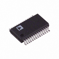
ADM560JRSZ Analog Devices Inc, ADM560JRSZ Datasheet - Page 3

ADM560JRSZ
Manufacturer Part Number
ADM560JRSZ
Description
IC TXRX RS232 4:5 3.3V LP 28SSOP
Manufacturer
Analog Devices Inc
Type
Transceiverr
Datasheet
1.ADM560JRZ-REEL.pdf
(12 pages)
Specifications of ADM560JRSZ
Number Of Drivers/receivers
4/5
Protocol
RS232
Voltage - Supply
3 V ~ 3.6 V
Mounting Type
Surface Mount
Package / Case
28-SSOP
Data Rate
116Kbps
Interface Circuit Standard 1
EIA-232/RS-232
Number Of Receivers
5
Number Of Transmitters
4
Number Of Transceivers
1
Data Transmission Topology
Point-to-Point
Receiver Signal Type
Single-Ended
Transmitter Signal Type
Single-Ended
Single Supply Voltage (typ)
3.3V
Single Supply Voltage (min)
3V
Single Supply Voltage (max)
3.6V
Dual Supply Voltage (typ)
Not RequiredV
Dual Supply Voltage (min)
Not RequiredV
Dual Supply Voltage (max)
Not RequiredV
Supply Current
5mA
Power Supply Requirement
Single
Operating Temp Range
0C to 70C
Operating Temperature Classification
Commercial
Mounting
Surface Mount
Pin Count
28
Package Type
SSOP
Lead Free Status / RoHS Status
Lead free / RoHS Compliant
Available stocks
Company
Part Number
Manufacturer
Quantity
Price
Part Number:
ADM560JRSZ
Manufacturer:
ADI/亚德诺
Quantity:
20 000
Part Number:
ADM560JRSZ-REEL
Manufacturer:
ADI/亚德诺
Quantity:
20 000
SPECIFICATIONS
V
Table 1.
Parameter
Output Voltage Swing
V
Shutdown Supply Current
Input Logic Threshold Low, V
Input Logic Threshold High, V
Logic Pull-Up Current
EIA-232 Input Voltage Range
EIA-232 Input Threshold Low
EIA-232 Input Threshold High
EIA-232 Input Hysteresis
EIA-232 Input Resistance
CMOS Output Voltage Low, V
CMOS Output Voltage High, V
CMOS Output Leakage Current
Output Enable Time
Output Disable Time
Receiver Propagation Delay
Transition Region Slew Rate
Transmitter Output Resistance
RS-232 Output Short-Circuit Current
CC
CC
TPHL
TPLH
Power Supply Current
= +3.3 V ± 10%, C1 to C4 = 1 μF, all specifications T
INL
OL
INH
OH
Min
±5.0
±4
2.4
–25
0.4
3
2.8
300
Typ
±5.5
±4.5
3.5
3.5
0.2
3
0.8
1.1
0.3
5
+0.05
100
50
0.1
0.5
4.5
±10
MIN
Max
5
5
5
0.4
20
+25
2.4
7
0.4
±5
1
2
to T
Rev. B | Page 3 of 12
MAX
Unit
V
V
mA
mA
μA
V
V
μA
V
V
V
V
kΩ
V
V
μA
ns
ns
μs
μs
V/μs
Ω
mA
, unless otherwise noted.
Test Conditions/Comments
V
V
No load, T
No load, T
SHDN = GND (ADM560), SHDN = V
T
T
T
I
I
EN = V
R
−3 V to +3 V
V
OUT
OUT
IN
IN
IN
CC
CC
L
CC
, EN, EN , SHDN, SHDN
, EN, EN, SHDN, SHDN
= 3 kΩ, C
= GND
= 3.3 V, three transmitter outputs loaded with 3 kΩ to ground
= 3.0 V, all transmitter outputs, loaded with 3 kΩ to ground
= V+ = V− = 0 V, V
= 1.6 mA
= −40 mA
CC
, EN = GND, 0 V ≤ R
IN
IN
L
= V
= GND
= 2500 pF measured from +3 V to −3 V or
CC
OUT
= ±2 V
OUT
≤ V
CC
ADM560/ADM561
CC
(ADM561), T
IN
= V
CC


