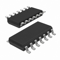
TJA1055T/C,512 NXP Semiconductors, TJA1055T/C,512 Datasheet - Page 14

TJA1055T/C,512
Manufacturer Part Number
TJA1055T/C,512
Description
IC CAN TXRX FAULT-TOL 14-SOIC
Manufacturer
NXP Semiconductors
Type
Transceiverr
Datasheet
1.TJA1055T3C518.pdf
(26 pages)
Specifications of TJA1055T/C,512
Package / Case
14-SOIC (3.9mm Width), 14-SOL
Number Of Drivers/receivers
1/1
Protocol
CAN
Voltage - Supply
4.75 V ~ 5.25 V
Mounting Type
Surface Mount
Product
Controller Area Network (CAN)
Number Of Transceivers
1
Data Rate
125 KBd
Supply Voltage (max)
5.25 V, 40 V
Supply Voltage (min)
4.75 V, 5 V
Supply Current (max)
0.22 mA, 21 mA
Maximum Operating Temperature
+ 125 C
Minimum Operating Temperature
- 40 C
Mounting Style
SMD/SMT
Lead Free Status / RoHS Status
Lead free / RoHS Compliant
Other names
935285398512
TJA1055T/C
TJA1055T/C
TJA1055T/C
TJA1055T/C
Available stocks
Company
Part Number
Manufacturer
Quantity
Price
Company:
Part Number:
TJA1055T/C,512
Manufacturer:
INFINEON
Quantity:
12 000
NXP Semiconductors
Table 8.
V
ground; positive currents flow into the device; unless otherwise specified.
[1]
11. Dynamic characteristics
Table 9.
V
ground; unless otherwise specified.
TJA1055_4
Product data sheet
Symbol
R
R
Pins RTH and RTL
R
R
V
I
I
I
Thermal shutdown
T
Symbol
t
t
t
O(RTL)
pu(RTL)
pd(RTH)
t(reces-dom)
t(dom-reces)
PD(L)
CC
CC
j(sd)
O(RTH)
i(se)(CANL)
i(dif)
sw(RTL)
sw(RTH)
= 4.75 V to 5.25 V; V
All parameters are guaranteed over the virtual junction temperature range by design, but only 100 % tested at T
wafer level, and above this for cased products 100 % tested at T
= 4.75 V to 5.25 V; V
Static characteristics
Dynamic characteristics
Parameter
transition time for recessive to
dominant (on pins CANL and
CANH)
transition time for dominant to
recessive (on pins CANL and
CANH)
propagation delay TXD (LOW) to
RXD (LOW)
Parameter
single-ended input
resistance on pin CANL
differential input
resistance
switch-on resistance on
pin RTL
switch-on resistance on
pin RTH
output voltage on pin RTH low power modes; I
output current on pin RTL low power modes; V
pull-up current on pin RTL normal operating mode and
pull-down current on
pin RTH
shutdown junction
temperature
BAT
BAT
= 5.0 V to 40 V; V
= 5.0 V to 40 V; V
…continued
[1]
Conditions
normal operating mode
normal operating mode
normal operating mode; switch-on
resistance between pin RTL and
V
normal operating mode; switch-on
resistance between pin RTH and
ground; I
failures 4, 6 and 7
normal operating mode and
failures 3 and 3a
CC
STB
STB
; I
Rev. 04 — 17 February 2009
Conditions
between 10 % and 90 %; R
125 ; C
see
between 10 % and 90 %; R
125 ; C
see
no failures; R
C
Figure 6
all failures except CAN_L shorted to CAN_H;
R
C
failure 7, CAN_L shorted to CAN_H;
R
C
Figure 6
O
= V
= V
CAN_L
CAN_L
CAN_H
CAN_L
CAN_L
< 10 mA
O
Figure 5
Figure 5
CC
CC
< 10 mA
; T
; T
= C
= R
= 1 M ; R
= C
= 1 nF; see
CAN_L
CAN_L
vj
vj
CAN_H
CAN_H
CAN_H
= 40 C to +150 C; all voltages are defined with respect to
= 40 C to +150 C; all voltages are defined with respect to
amb
O
and
and
CAN_L
RTL
= 100 A
= C
= C
= 25 C, unless otherwise specified.
6
6
= 1 nF; see
= 125 ; C
= 1 nF; see
= 0 V
CAN_H
CAN_H
CAN_H
= R
Figure 4
CAN_H
[1]
= 125 ;
= 1 nF;
= 1 nF;
Enhanced fault-tolerant CAN transceiver
CAN_L
CAN_L
CAN_L
to
= 125 ;
Figure 4
Figure 4
Figure 6
= R
= R
Min
110
220
-
-
-
-
-
160
=
1.5
CAN_H
CAN_H
to
to
=
=
Typ
165
330
40
40
0.7
75
75
175
0.65
Min Typ Max Unit
0.2
0.3
-
-
-
amb
© NXP B.V. 2009. All rights reserved.
TJA1055
= 125 C for dies on
0.6
0.7
-
-
-
Max
270
540
100
100
1.0
-
-
190
0.1
-
-
1.5
1.9
1.9
14 of 26
Unit
k
k
V
mA
C
A
A
s
s
s
s
s


