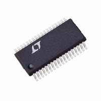
LTC1545CG#PBF Linear Technology, LTC1545CG#PBF Datasheet - Page 5

LTC1545CG#PBF
Manufacturer Part Number
LTC1545CG#PBF
Description
IC TXRX SOFTWARE SELECT 36-SSOP
Manufacturer
Linear Technology
Type
Transceiverr
Datasheet
1.LTC1545CGTR.pdf
(16 pages)
Specifications of LTC1545CG#PBF
Number Of Drivers/receivers
5/5
Voltage - Supply
4.75 V ~ 5.25 V
Mounting Type
Surface Mount
Package / Case
36-SSOP
Lead Free Status / RoHS Status
Lead free / RoHS Compliant
Protocol
-
Available stocks
Company
Part Number
Manufacturer
Quantity
Price
PIN
V
4.75V V
V
nect to V
capacitor to ground.
D1 (Pin 3): TTL Level Driver 1 Input.
D2 (Pin 4): TTL Level Driver 2 Input.
D3 (Pin 5): TTL Level Driver 3 Input.
R1 (Pin 6): CMOS Level Receiver 1 Output.
R2 (Pin 7): CMOS Level Receiver 2 Output.
R3 (Pin 8): CMOS Level Receiver 3 Output.
D4 (Pin 9): TTL Level Driver 4 Input.
R4 (Pin 10): CMOS Level Receiver 4 Output.
M0 (Pin 11): TTL Level Mode Select Input 0 with Pull-Up
to V
M1 (Pin 12): TTL Level Mode Select Input 1 with Pull-Up
to V
M2 (Pin 13): TTL Level Mode Select Input 2 with Pull-Up
to V
DCE/DTE (Pin 14): TTL Level Mode Select Input with
Pull-Up to V
enables Receiver 1.
D4ENB (Pin 15): TTL Level Enable Input with Pull-Up to
V
R4EN (Pin 16): TTL Level Enable Input with Pull-Up to V
Logic high enables Receiver 4.
TEST CIRCUITS
CC
DD
CC
U
. Logic low enables Driver 4.
CC
CC
CC
(Pins 1, 19): Positive Supply for the Transceivers.
(Pins 2, 20): Positive Supply Voltage for V.28. Con-
.
.
.
FUNCTIONS
DD
CC
U
Pin 3 on LTC1543 or 8V supply. Connect a 1 F
CC
5.25V. Connect a 1 F capacitor to ground.
Figure 1. V.11 Driver Test Circuit
. Logic high enables Driver 3. Logic low
A
B
U
V
OD
R
R
L
L
V
OC
1545 F01
CC
.
R5 (Pin 17): CMOS Level Receiver 5 Output.
D5 (Pin 18): TTL Level Driver 5 Input.
D5 A (Pin 21): Driver 5 Output.
R5 A (Pin 22): Receiver 5 Input.
R4 A (Pin 23): Receiver 4 Input.
D4 A (Pin 24): Driver 4 Input.
R3 B (Pin 25): Receiver 3 Noninverting Input.
R3 A (Pin 26): Receiver 3 Inverting Input.
R2 B (Pin 27): Receiver 2 Noninverting Input.
R2 A (Pin 28): Receiver 2 Inverting Input.
D3/R1 B (Pin 29): Receiver 1 Noninverting Input and
Driver 3 Noninverting Output.
D3/R1 A (Pin 30): Receiver 1 Inverting Input and Driver 3
Inverting Output.
D2 B (Pin 31): Driver 2 Noninverting Output.
D2 A (Pin 32): Driver 2 Inverting Output.
D1 B (Pin 33): Driver 1 Noninverting Output.
D1 A (Pin 34): Driver 1 Inverting Output.
GND (Pin 35): Ground.
V
26 on LTC1543. Connect a 1 F capacitor to ground.
EE
(Pin 36): Negative Supply Voltage. Connect to V
Figure 2. V.11 Driver/Receiver AC Test Circuit
B
A
R
100
L
C
100pF
C
100pF
L
L
B
A
LTC1545
R
15pF
1545 F02
EE
5
Pin


