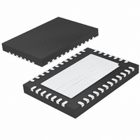
LTC2847CUHF Linear Technology, LTC2847CUHF Datasheet - Page 6

LTC2847CUHF
Manufacturer Part Number
LTC2847CUHF
Description
IC TXRX MULTIPROTOCOL 38-QFN
Manufacturer
Linear Technology
Type
Transceiverr
Datasheet
1.LTC2847IUHFPBF.pdf
(20 pages)
Specifications of LTC2847CUHF
Number Of Drivers/receivers
3/3
Protocol
Multiprotocol
Voltage - Supply
5V
Mounting Type
Surface Mount
Package / Case
38-QFN
Lead Free Status / RoHS Status
Contains lead / RoHS non-compliant
Available stocks
Company
Part Number
Manufacturer
Quantity
Price
Company:
Part Number:
LTC2847CUHF
Manufacturer:
LT
Quantity:
10 000
Part Number:
LTC2847CUHF
Manufacturer:
LINEAR/凌特
Quantity:
20 000
Part Number:
LTC2847CUHF#TRPBF
Manufacturer:
LINEAR/凌特
Quantity:
20 000
PI FU CTIO S
LTC2847
NC (Pins 1,3,18,19,22,23): No Connect.
V
V.28. Connect a 1 F capacitor to ground.
V
pump and transceiver. 4.75V V
1 F capacitor to GND.
D1 (Pin 5): TTL Level Driver 1 Input.
D2 (Pin 6): TTL Level Driver 2 Input.
D3 (Pin 7): TTL Level Driver 3 Input.
R1 (Pin 8): CMOS Level Receiver 1 Output with Pull-Up to
V
R2 (Pin 9): CMOS Level Receiver 2 Output with Pull-Up to
V
R3 (Pin 10): CMOS Level Receiver 3 Output with Pull-Up
to V
M0 (Pin 11): TTL Level Mode Select Input 0 with Pull-Up
to V
M1 (Pin 12): TTL Level Mode Select Input 1 with Pull-Up
to V
V
interface including receiver output drivers. 3V
5.25V. Connect to V
lower receiver output swing. Connect a 1 F capacitor to
GND.
M2 (Pin 14): TTL Level Mode Select Input 2 with Pull-Up
to V
DCE/DTE (Pin 15): TTL Level Mode Select Input with
Pull-Up to V
6
DD
CC
IN
IN
IN
U
when Three-Stated.
when Three-Stated.
IN
IN
IN
IN
(Pin 13): Input Supply Pin. Input supply to digital
(Pin 4): Input Supply Pin. Input supply to charge
(Pin 2): Generated Positive Supply Voltage for
. See Table 1.
. See Table 1.
. See Table 1.
when Three-Stated.
U
IN
. See Table 1.
U
CC
(Pin 4) or to separate supply for
CC
5.25V. Connect a
V
IN
R3 B (Pin 16): Receiver 3 Noninverting Input.
R3 A (Pin 17): Receiver 3 Inverting Input.
R2 B (Pin 20): Receiver 2 Noninverting Input.
R2 A (Pin 21): Receiver 2 Inverting Input.
D3/R1 B (Pin 24): Receiver 1 Noninverting Input and
Driver 3 Noninverting Output.
D3/R1 A (Pin 25): Receiver 1 Inverting Input and Driver 3
Inverting Output.
D2 B (Pin 26): Driver 2 Noninverting Output.
D2 A (Pin 27): Driver 2 Inverting Output.
D1 B (Pin 28): Driver 1 Noninverting Output.
D1 A (Pin 29): Driver 1 Inverting Output.
GND (Pins 30,31): Transceiver Ground.
V
Connect a 3.3 F capacitor to GND. Exposed pad can also
be connected to V
C2
1 F capacitor between C2
C2
1 F capacitor between C2
C1
1 F capacitor between C1
C1
1 F capacitor between C1
EE
–
+
–
+
(Pins 32,33,36): Generated Negative Supply Voltage.
(Pin 37): Capacitor C1 Negative Terminal. Connect a
(Pin 38): Capacitor C1 Positive Terminal. Connect a
(Pin 34): Capacitor C2 Negative Terminal. Connect a
(Pin 35): Capacitor C2 Positive Terminal. Connect a
EE
.
+
+
+
+
and C1
and C1
and C2
and C2
–
–
–
–
.
.
.
.
sn2847 2847fs


