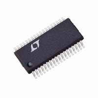
LTC1545IG#TR Linear Technology, LTC1545IG#TR Datasheet - Page 7

LTC1545IG#TR
Manufacturer Part Number
LTC1545IG#TR
Description
IC TXRX SOFTWARE SELECTBL 36SSOP
Manufacturer
Linear Technology
Type
Transceiverr
Datasheet
1.LTC1545CGTR.pdf
(16 pages)
Specifications of LTC1545IG#TR
Number Of Drivers/receivers
5/5
Voltage - Supply
4.75 V ~ 5.25 V
Mounting Type
Surface Mount
Package / Case
36-SSOP
Lead Free Status / RoHS Status
Contains lead / RoHS non-compliant
Protocol
-
Available stocks
Company
Part Number
Manufacturer
Quantity
Price
SWITCHI G TI E WAVEFOR S
APPLICATIONS
Overview
The LTC1543/LTC1545 form the core of a complete soft-
ware-selectable DTE or DCE interface port that supports
the RS232, RS449, EIA530, EIA530-A, V.35, V.36 or X.21
protocols. Cable termination may be implemented using
the LTC1344A software-selectable cable termination chip
or by using existing discrete designs.
A complete DCE-to-DTE interface operating in EIA530
mode is shown in Figure 9. The LTC1543 of each port is
used to generate the clock and data signals. The LTC1545
is used to generate the control signals along with LL (Local
Loop-Back), RL (Remote Loop-Back), TM (Test Mode)
and RI (Ring Indicate). The LTC1344A cable termination
chip is used only for the clock and data signals because
they must support V.35 cable termination. The control
signals do not need any external resistors.
B – A
–V
R
A
V
R
D
A
V
V
V
OD2
OD2
V
–V
V
V
OH
OH
OL
OL
3V
0V
V
IH
IL
O
O
U
U
W
INFORMATION
U
1.5V
0V
1.5V
t
t
PHL
PLH
t
PHL
3V
W
t
Figure 8. V.10, V.28 Receiver Propagation Delays
1.5V
f
1.5V
Figure 7. V.10, V.28 Driver Propagation Delays
0V
Figure 6. V.11 Receiver Propagation Delays
–3V
W
f = 1MHz : t
U
r
10ns : t
Mode Selection
The interface protocol is selected using the mode select
pins M0, M1 and M2 (see the Mode Selection table).
For example, if the port is configured as a V.35 interface,
the mode selection pins should be M2 = 1, M1 = 0, M0 = 0.
For the control signals, the drivers and receivers will
operate in V.28 (RS232) electrical mode. For the clock and
data signals, the drivers and receivers will operate in V.35
electrical mode. The DCE/DTE pin will configure the port
for DCE mode when high, and DTE when low.
The interface protocol may be selected simply by plugging
the appropriate interface cable into the connector. The
mode pins are routed to the connector and are left uncon-
nected (1) or wired to ground (0) in the cable as shown in
Figure 10.
f
10ns
OUTPUT
INPUT
1.5V
0V
1.5V
t
–3V
PLH
t
t
PHL
PLH
0V
t
r
1.5V
1.5V
3V
LTC1545
1545 F08
1545 F06
1545 F07
7


