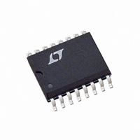
LTC489ISW#PBF Linear Technology, LTC489ISW#PBF Datasheet - Page 5

LTC489ISW#PBF
Manufacturer Part Number
LTC489ISW#PBF
Description
IC LINE RCVR RS485 QUAD 16-SOIC
Manufacturer
Linear Technology
Type
Line Receiverr
Datasheet
1.LTC488CNPBF.pdf
(12 pages)
Specifications of LTC489ISW#PBF
Number Of Drivers/receivers
0/4
Protocol
RS422, RS485
Voltage - Supply
4.75 V ~ 5.25 V
Mounting Type
Surface Mount
Package / Case
16-SOIC (0.300", 7.5mm Width)
Interface Circuit Standard 1
RS-485
Number Of Receivers
4
Number Of Transmitters
Not Required
Number Of Transceivers
Not Required
Data Transmission Topology
Multipoint
Receiver Signal Type
Differential
Transmitter Signal Type
Not Required
Single Supply Voltage (typ)
5V
Single Supply Voltage (min)
4.75V
Single Supply Voltage (max)
5.25V
Dual Supply Voltage (typ)
Not RequiredV
Dual Supply Voltage (min)
Not RequiredV
Dual Supply Voltage (max)
Not RequiredV
Supply Current
10mA
Power Supply Requirement
Single
Operating Temp Range
-40C to 85C
Operating Temperature Classification
Industrial
Mounting
Surface Mount
Pin Count
16
Package Type
SOIC W
Lead Free Status / RoHS Status
Lead free / RoHS Compliant
Available stocks
Company
Part Number
Manufacturer
Quantity
Price
PIN FUNCTIONS
B 1 (Pin 1): Receiver 1 Input.
A1 (Pin 2): Receiver 1 Input.
RO1 (Pin 3): Receiver 1 Output. If the receiver output
is enabled, then if A > B by 200mV, RO1 will be high. If
A < B by 200mV, then RO1 will be low.
EN (Pin 4) LTC488: Receiver Output Enabled. See Function
Table for details.
EN12 (Pin 4) LTC489: Receiver 1, Receiver 2 Output
Enabled. See Function Table for details.
RO2 (Pin 5): Receiver 2 Output. Refer to RO1.
A2 (Pin 6): Receiver 2 Input.
B2 (Pin 7): Receiver 2 Input.
FUNCTION TABLES
LTC488
DIFFERENTIAL
A – B
V
–0.2V < V
V
X
ID
ID
≥ 0.2V
≤ 0.2V
ID
< 0.2V
EN
H
X
H
X
H
X
L
ENABLES
EN
X
X
X
H
L
L
L
OUTPUT
RO
H
H
?
?
L
L
Z
GND (Pin 8): Ground Connection.
B3 (Pin 9): Receiver 3 Input.
A3 (Pin 10): Receiver 3 Input.
RO3 (Pin 11): Receiver 3 Output. Refer to RO1.
EN (Pin 12) LTC488: Receiver Output Disabled. See Func-
tion Table for details.
EN34 (Pin 12) LTC489: Receiver 3, Receiver 4 output
enabled. See Function Table for details.
RO4 (Pin 13): Receiver 4 Output. Refer to RO1.
A4 (Pin 14): Receiver 4 Input.
B4 (Pin 15): Receiver 4 Input.
V
LTC489
DIFFERENTIAL
A – B
V
–0.2V < V
V
X
H: High Level
L: Low Level
X: Irrelevant
ID
ID
CC
≥ 0.2V
≤ 0.2V
(Pin 16): Positive Supply; 4.75V ≤ V
ID
< 0.2V
LTC488/LTC489
?: Indeterminate
Z: High Impedance (Off)
EN12 or EN34
ENABLES
H
H
H
L
CC
≤ 5.25V.
OUTPUT
RO
H
?
L
Z
4889fb
5


