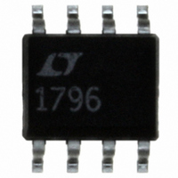
LT1796CS8 Linear Technology, LT1796CS8 Datasheet - Page 5

LT1796CS8
Manufacturer Part Number
LT1796CS8
Description
IC CAN TXRX VOLT FAULT PROT8SOIC
Manufacturer
Linear Technology
Type
Transceiverr
Datasheet
1.LT1796CS8PBF.pdf
(8 pages)
Specifications of LT1796CS8
Number Of Drivers/receivers
1/1
Protocol
CAN
Voltage - Supply
4.75 V ~ 5.25 V
Mounting Type
Surface Mount
Package / Case
8-SOIC (3.9mm Width)
Lead Free Status / RoHS Status
Contains lead / RoHS non-compliant
Available stocks
Company
Part Number
Manufacturer
Quantity
Price
Part Number:
LT1796CS8
Manufacturer:
LT/凌特
Quantity:
20 000
Company:
Part Number:
LT1796CS8#PBF
Manufacturer:
MICREL
Quantity:
235
Part Number:
LT1796CS8#PBF
Manufacturer:
LINEAR/凌特
Quantity:
20 000
Part Number:
LT1796CS8#TRPBF
Manufacturer:
LINEAR/凌特
Quantity:
20 000
PI FU CTIO S
TYPICAL PERFOR A CE CHARACTERISTICS
TXD (Pin 1): Driver Input. Logic-level thresholds are set by
V
outputs off, releasing control of the CANH and CANL lines.
A logic input less than V
pulling CANH high and CANL low. An open TXD input will
float high, turning the driver outputs off. The TXD input pin
can withstand voltages from – 0.3V to 44V with no dam-
age.
GND (Pin 2): Ground.
V
with a 4.75V to 5.25V supply. Operation with supplies up
to 44V is possible with unterminated bus lines. Operation
at high voltages with normally terminated busses will
result in excessive power dissipation and activation of the
thermal shutdown circuit. V
a 0.1 F low ESR capacitor placed as close to the supply pin
as possible.
RXD (Pin 4): Receiver TTL Level-Logic Output. A high level
output indicates a recessive state (zero-volt differential)
bus. A dominant state forces a low receiver output.
V
the TXD input threshold and the recessive bus common
mode voltage at CANH and CANL. V
V
maintains a 3.5V level.
REF
CC
REF
CC
U
/2 for low voltage operation. When V
(Pin 3): Positive Supply Input. Normal operation is
. A logic input level higher than V
(Pin 5): Reference Output. The reference voltage sets
U
0.80
0.75
0.70
0.65
0.60
–50
Receiver Thresholds vs
Temperature
U
–25
REF
V
TH
W
TEMPERATURE ( C)
CC
RISING
0
turns the driver outputs on,
should be decoupled with
U
25
V
TH
REF
REF
FALLING
50
is approximately
CC
turns the driver
75
> 7.5V, V
1796 G10
100
REF
CANL (Pin 6): CAN Bus Low Data Line. The CANL pin is one
input to the receiver and the low driver output. In the
dominant state (TXD low), the driver pulls the CANL pin to
within 1V of GND. In the recessive state (TXD high), the
driver output stays high impedance. The CANL pin is
protected from voltage faults from – 60V to 60V in domi-
nant, recessive, standby or powered off modes. On-chip
ESD protection meets IEC-1000-4-2 levels.
CANH (Pin 7): CAN Bus High Data Line. The CANH pin is
one input to the receiver and the high driver output. In the
dominant state (TXD low), the driver pulls the CANH pin to
within 1V of V
driver output stays high impedance. The CANH pin is
protected from voltage faults from – 60V to 60V in domi-
nant, recessive, standby or powered off modes. On-chip
ESD protection meets IEC-1000-4-2 levels.
R
control pin. When R
into a low power standby mode. In standby, the driver
always stays in a high impedance (recessive) state. The
receiver operates in a low power (slow) monitoring mode.
Received data may be used to “wake-up” the system to full
functionality. Full speed normal operation occurs if R
tied low through a resistance of less than 3k. The current
out of R
Controlling the current out of R
than 3k or by using a current source allows slew rate
control of the data output onto CANH and CANL.
S
(Pin 8): Slope Control. This pin is a multifunction
S
400
350
300
250
200
will be limited to about 500 A in the low state.
–50
Receiver Propagation Delay vs
Temperature
CC
–25
. In the recessive state (TXD high), the
S
TEMPERATURE ( C)
t
0
is high (V
RXDOFF
25
t
RXDON
50
RS
S
with a resistor greater
> 4V), the circuit goes
75
1796 G11
100
LT1796
5
S
1796f
is


