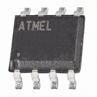
ATA6620N-TAQY Atmel, ATA6620N-TAQY Datasheet - Page 17

ATA6620N-TAQY
Manufacturer Part Number
ATA6620N-TAQY
Description
TXRX LIN BUS W/VREG SO-8
Manufacturer
Atmel
Type
Transceiverr
Datasheet
1.ATA6620N-TAQY.pdf
(22 pages)
Specifications of ATA6620N-TAQY
Protocol
LIN
Voltage - Supply
5 V ~ 18 V
Mounting Type
Surface Mount
Package / Case
SO-8
Number Of Transmitters
1
Number Of Receivers
1
Power Supply Requirement
Single
Operating Temperature Classification
Automotive
Mounting
Surface Mount
Pin Count
8
Operating Temperature (max)
125C
Operating Temperature (min)
-40C
Dual Supply Voltage (typ)
Not RequiredV
Dual Supply Voltage (max)
Not RequiredV
Dual Supply Voltage (min)
Not RequiredV
Lead Free Status / RoHS Status
Lead free / RoHS Compliant
Number Of Drivers/receivers
-
Lead Free Status / Rohs Status
Compliant
Available stocks
Company
Part Number
Manufacturer
Quantity
Price
Company:
Part Number:
ATA6620N-TAQY
Manufacturer:
ATMEL
Quantity:
5 000
Part Number:
ATA6620N-TAQY
Manufacturer:
ATMEL/爱特梅尔
Quantity:
20 000
8. Electrical Characteristics (Continued)
5V < V
4850I–AUTO–09/09
*) Type means: A = 100% tested, B = 100% correlation tested, C = Characterized on samples, D = Design parameter
10.1
10.2
10.3
10.4
10.5
10.6
10.7
10.8
11.1
11.2
No.
9.5
9.6
10
11
S
< 18V, T
Parameters
Wake detection LIN
High level input voltage
Wake detection LIN
Low level input voltage
Internal Timers
Dominant time for
wake–up via LIN bus
Time delay for mode
change from Pre-normal
into Normal mode via
pin EN
Time delay for mode
change from Normal
mode to Sleep mode via
pin EN
TXD dominant time out
timer
Duty cycle 1
Duty cycle 2
Slope time falling and
rising edge at LIN
Time delay for mode
change from Silent- into
Normal mode via EN
Receiver Electrical AC Parameters of the LIN Physical Layer
LIN Receiver, RXD Load Conditions (C
Propagation delay of
receiver Switch to Sleep
mode (see
page
Symmetry of receiver
propagation delay rising
edge minus falling edge
18)
amb
= –40°C to 125°C
Figure 8-1 on
Test Conditions
I
V
V
V
V
TH
TH
V
t
D1 = t
TH
TH
V
t
D2 = t
VEN = 5V
t
t
LIN
Bit
Bit
rx_pd
rx_sym
LIN
EN
EN
TXD
S
S
Rec(max)
Dom(max)
= 7.0V to 18V;
= 50 ms
Rec(min)
Dom(min)
= 7.0V to 18V;
= 50ms
= typically –3 mA
= 5V
= 0V
= 0V
= max(t
= 0V
bus_rec(min)
bus_rec(max)
= t
rx_pdr
= 0.422
= 0.744
= 0.284
= 0.581
rx_pdr
– t
/(2
RXD
/(2
rx_pdf
, t
): 20 pF; R
rx_pdf
V
t
V
V
t
V
Bit
Bit
S
S
S
S
;
)
;
)
;
)
;
Pin
LIN
LIN
pull-up
= 2.4 k
t
t
Symbol
SLOPE_rise
SLOPE_fall
t
V
V
t
rx_sym
t
t
t
rx_pd
t
norm
sleep
t
D1
D2
dom
LINH
LINL
bus
s_n
V
0.396
S
Min.
–27
3.5
30
–2
– 1V
5
2
6
5
Typ.
90
10
15
7
V
V
S
S
0.581
Max.
22.5
150
+ 0.3V
– 3.3V
20
15
20
40
+2
6
ATA6620N
Unit
ms
µs
µs
µs
µs
µs
µs
µs
V
V
Type*
A
A
A
A
A
A
A
A
A
A
A
A
17


