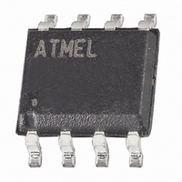
ATA6661-TAQJ 19 Atmel, ATA6661-TAQJ 19 Datasheet - Page 9

ATA6661-TAQJ 19
Manufacturer Part Number
ATA6661-TAQJ 19
Description
TXRX LIN 2.0 3.3V/5V 8SOIC
Manufacturer
Atmel
Type
Transceiverr
Datasheet
1.ATA6661-TAQJ_19.pdf
(16 pages)
Specifications of ATA6661-TAQJ 19
Number Of Drivers/receivers
1/1
Protocol
LIN
Voltage - Supply
3.3V, 5V
Mounting Type
Surface Mount
Package / Case
SO-8
Number Of Transmitters
1
Number Of Receivers
1
Power Supply Requirement
Single
Package Type
SO
Operating Temperature Classification
Automotive
Mounting
Surface Mount
Pin Count
8
Operating Temperature (max)
125C
Operating Temperature (min)
-40C
Dual Supply Voltage (typ)
Not RequiredV
Dual Supply Voltage (max)
Not RequiredV
Dual Supply Voltage (min)
Not RequiredV
Maximum Operating Temperature
+ 125 C
Minimum Operating Temperature
- 40 C
Mounting Style
SMD/SMT
Operating Supply Voltage
- 0.3 V to + 40 V
Propagation Delay Time Ns
6 us
Supply Current
1.6 mA
Lead Free Status / RoHS Status
Lead free / RoHS Compliant
6. Electrical Characteristics
5V < V
4729M–AUTO–02/09
*) Type means: A = 100% tested, B = 100% correlation tested, C = Characterized on samples, D = Design parameter
No.
1.1
1.2
1.3
1.4
1.5
1.6
2.1
2.2
2.3
2.4
3.1
3.2
3.3
3.4
3.5
4.1
4.2
4.3
4.4
4.5
5.1
5.2
6.1
6.2
1
2
3
4
5
6
S
< 18V, T
Parameters
V
Nominal DC voltage range
Supply current in sleep mode
Supply current in normal mode
V
V
hysteresis
RXD Output Pin (Open Drain)
Low level input current
RXD saturation voltage
High level leakage current
ESD zener diode
TXD Input Pin
Low level voltage input
High level voltage input
Pull-down resistor
Low level leakage current
Low-level input current at local
wake-up request
EN Input Pin
Low level voltage input
High level voltage input
Pull-down resistor
Low level input current
Enable negative slope for go to
sleep
INH Output Pin
High level voltage
High level leakage current
WAKE Pin
High level input voltage
Low level input voltage
S
S
S
Pin
undervoltage threshold
undervoltage threshold
amb
= –40°C to +125°C
Test Conditions
Sleep mode
V
V
Bus recessive
Bus dominant
Total bus load > 500
Normal mode
V
5 k pull-up resistor to 5V
Normal mode
V
I
V
V
Pre-normal mode
V
V
V
Negative slope
V
Normal mode
I
Sleep mode
V
I
RXD
INH
WAKE
lin
Batt
LIN
LIN
TXD
TXD
LIN
EN
EN
EN
INH
> V
= –200 µA
= 5V
= 0V
= 2V to 0.8V
= 0V, V
= V
= V
= 100 µA
= 27V, V
< 14V
= 5V
= 0V
= Typically –3 µA
Batt
BAT
BAT
, V
– 0.5V
; V
RXD
Batt
RXD
WAKE
= 0.4V
= 27V
= 5V
= 0V
Pin
7
7
7
7
7
1
1
1
1
4
4
4
4
4
2
2
2
2
2
8
8
3
3
Symbol
Slope
Vsat
I
V
V
V
VZ
TXDwake
I
I
V
V
V
I
I
I
R
V
VSdom
V
VSstby
Sth_hys
I
WAKEH
V
RXDH
R
WAKEL
VSrec
RXDL
I
INHL
TXDH
I
V
TXDL
TXD
INHH
ENH
TXD
ENL
EN
Sth
EN
RXD
S
RXD
EN
V
S
–27V
Min.
–0.3
–0.3
V
125
125
6.1
–3
–3
–3
–3
1V
– 0.8
S
5
4
2
2
2
2
–
Typ.
13.5
250
250
1.6
1.6
4.6
0.2
10
5
5
Max.
0.3V
+0.8
+0.8
V
V
600
600
0.4
8.6
3V
18
20
+3
+3
+3
60
V
+3
S
S
3
3
5
8
6
8
6
S
+
–
ATA6661
Unit
mA
mA
mA
mA
µA
µA
k
µA
k
µA
µA
µs
V
V
V
V
V
V
V
V
V
V
V
V
Type*
A
A
A
A
A
A
A
A
A
A
A
A
A
A
A
A
A
A
A
A
A
A
A
A
9


