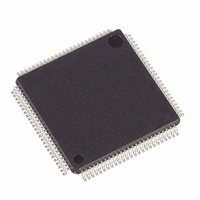
DS2154L Maxim Integrated Products, DS2154L Datasheet - Page 13

DS2154L
Manufacturer Part Number
DS2154L
Description
IC TXRX E1 1CHIP 5V ENH 100-LQFP
Manufacturer
Maxim Integrated Products
Type
Transceiverr
Datasheet
1.DS2154L.pdf
(87 pages)
Specifications of DS2154L
Number Of Drivers/receivers
1/1
Protocol
E1
Voltage - Supply
4.75 V ~ 5.25 V
Mounting Type
Surface Mount
Package / Case
100-LQFP
Lead Free Status / RoHS Status
Contains lead / RoHS non-compliant
Available stocks
Company
Part Number
Manufacturer
Quantity
Price
Part Number:
DS2154L
Manufacturer:
DALLAS
Quantity:
20 000
Part Number:
DS2154L+
Manufacturer:
DALLAS
Quantity:
20 000
2.3 Parallel Control Port Pins
56–65
66–72
PIN
PIN
93
91
90
89
86
87
88
25
14
55
11
74
75
73
77
6
3
AD0–AD7
WR(R/W)
ALE(AS)
RD(DS)
D0–D7/
8MCLK
RNEGO
RCLKO
RPOSO
A0–A6
NAME
RNEGI
RCLKI
NAME
RSIGF
RPOSI
MUX
TEST
BTS
RCL
INT
CS
Bus Operation. Set low to select nonmultiplexed bus operation. Set high to select
multiplexed bus operation.
Data Bus or Address/Data Bus. In nonmultiplexed bus operation (MUX = 0), serves as
the data bus. In multiplexed bus operation (MUX = 1), serves as an 8-bit multiplexed
address/data bus.
Address Bus. In nonmultiplexed bus operation (MUX = 0), serves as the address bus. In
multiplexed bus operation (MUX = 1), these pins are not used and should be tied low.
Bus Type Select. Strap high to select Motorola bus timing; strap low to select Intel bus
timing. This pin controls the function of the
If BTS = 1, then these pins assume the function listed in parentheses.
Read Input (Data Strobe).
active high when MUX = 0. See the bus timing diagrams.
Chip Select. Must be low to read or write to the device.
A7 or Address Latch Enable (Address Strobe). In nonmultiplexed bus operation
(MUX = 0), serves as the upper address bit. In multiplexed bus operation (MUX = 1),
serves to demultiplex the bus on a positive-going edge.
Write Input (Read/Write).
Interrupt. Flags host controller during conditions and change of conditions defined in
the Status Registers 1 and 2. Active-low, open-drain output.
Tri-State Control. Set high to tri-state all output and I/O pins (including the parallel
control port). Set low for normal operation. Useful in board-level testing.
controlled by the TCR2.0 control bit. This pin can be programmed to either toggle high
when the synchronizer is searching for the frame and multiframe or to toggle high if the
TCLK pin has not been toggled for 5µs.
Receive Carrier Loss. Set high when the line interface detects a loss of carrier. Note: A
test mode exists to allow the DS2154 to detect carrier loss at RPOSI and RNEGI in
place of detection at RTIP and RRING.
Receive Signaling Freeze. Set high when the signaling data is frozen via either
automatic or manual intervention. Used to alert downstream equipment of the condition.
8MHz Clock. A 8.192MHz output clock that is referenced to the clock that is output at
the RCLK pin.
Receive Positive Data Output. Updated on the rising edge of RCLKO with the bipolar
data out of the line interface. This pin is normally tied to RPOSI.
Receive Negative Data Output. Updated on the rising edge of RCLKO with the bipolar
data out of the line interface. This pin is normally tied to RNEGI.
Receive Clock Output. Buffered recovered clock from the E1 line. This pin is normally
tied to RCLKI.
Receive Positive Data Input. Sampled on the falling edge of RCLKI for data to be
clocked through the receive side framer. RPOSI and RNEGI can be tied together for a
NRZ interface. Can be internally connected to RPOSO by tying the LIUC pin high.
Receive Negative Data Input. Sampled on the falling edge of RCLKI for data to be
clocked through the receive side framer. RPOSI and RNEGI can be tied together for a
NRZ interface. Can be internally connected to RNEGO by tying the LIUC pin high.
Receive Clock Input. Clock used to clock data through the receive side framer. This pin
is normally tied to RCLKO. Can be internally connected to RCLKO by tying the LIUC
pin high. RCLKI must be present for the parallel control port to operate properly.
13 of 87
RD
WR
and
is an active-low signal.
DS
FUNCTION
FUNCTION
are active-low signals when MUX = 1. DS is
RD
(
DS
), ALE(AS), and
CS
is an active-low signal.
WR
(R/
W
) pins.


