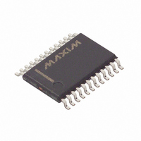
MAX3388EEUG+ Maxim Integrated Products, MAX3388EEUG+ Datasheet - Page 9

MAX3388EEUG+
Manufacturer Part Number
MAX3388EEUG+
Description
IC TXRX RS232 250KBPS 24-TSSOP
Manufacturer
Maxim Integrated Products
Type
Transceiverr
Datasheet
1.MAX3388EEUG.pdf
(11 pages)
Specifications of MAX3388EEUG+
Number Of Drivers/receivers
3/3
Protocol
RS232
Voltage - Supply
3 V ~ 5.5 V
Mounting Type
Surface Mount
Package / Case
24-TSSOP
Propagation Delay Time Ns
0.15 us
Operating Supply Voltage
2.35 V to 3 V
Supply Current
0.3 mA
Operating Temperature Range
- 40 C to + 85 C
Data Rate
460 Kbps
Mounting Style
SMD/SMT
Number Of I/os
3 / 2
Lead Free Status / RoHS Status
Lead free / RoHS Compliant
The MAX3388E/MAX3389E maintain RS-232-compatible
transmitter output voltages even at high data rates. Figure
5 shows a transmitter loopback test circuit. Figure 6 shows
a loopback test result at 250kbps, and Figure 7 shows the
same test at 460kbps. For Figure 6, all transmitters were
driven simultaneously at 250kbps into RS-232 loads in
parallel with 1000pF. For Figure 7, a single transmitter was
driven at 460kbps, and all transmitters were loaded with
an RS-232 receiver in parallel with 150pF.
The MAX3388E/MAX3389E contain an internal switch
for powering external circuitry. This can be used to
power hot-sync circuitry or other low-power circuitry.
The switch on- resistance is typically 62Ω. The SWIN
side of the switch is ESD protected to ±15kV.
In addition to the traditional RS-232 I/O, the
MAX3388E/MAX3389E have a logic-level transceiver
from the RS-232 connector side to the CMOS-logic
side. The input impedance is typically 30kΩ, and the
output is open drain. The logic level I/O is active during
shutdown for the MAX3389E.
This I/O transceiver is useful for hot syncing or other
dedicated communication capability. The input is ESD
protected to ±15kV.
The MAX3388E/MAX3389E designed with PDA applica-
tions in mind. Two transmitters and two receivers handle
standard full-duplex communication protocol, while an
extra transmitter allows a ring indicator (RI) signal to alert
the UART on the PC. Without the ring indicator transmit-
ter, solutions for these applications would require soft-
ware-intensive polling of the cradle inputs.
The RI signal is generated when a PDA, cellular phone, or
other “cradled” device is plugged into its cradle. This
generates a logic-low signal to RI transmitter input, creat-
ing +3.7V at the ring indicate pin. The PC’s UART RI input
is the only pin that can generate an interrupt from signals
arriving through the RS-232 port. The interrupt routine for
this UART will then service the RS-232 full-duplex com-
munication between the PDA and the PC.
As cell phone design becomes more like that of PDAs,
cell phones will require similar docking ability and com-
munication protocol. Cell phones operate on a single
lithium-ion (Li+) battery and generate a regulated out-
put voltage of +2.35V to +3V from the phone connector.
The baseband logic coming from the phone connector
can be as low as 1.8V at the transceivers. To prevent
forward biasing of a device internal to the cell phone,
the MAX3388E/MAX3389E come with a logic power-
supply pin (V
Typical PDA/Cell-Phone Application
L
) that limits the logic levels presented to
_______________________________________________________________________________________
Transceivers for PDAs and Cell Phones
2.5V, ±15kV ESD-Protected RS-232
High Data Rates
Logic-Level I/O
Power Switch
Figure 5. Loopback Test Circuit
Figure 6. Loopback Test Results at 250kbps
C1
C2
V
R1OUT
T1OUT
V
CC
T1IN
CC
0.1µF
SHDN
T_ IN
R_ OUT
C1+
C1-
C2+
C2-
MAX3388E
MAX3389E
1µs/div
GND
V
CC
C
L
T_ OUT
5kΩ
= 1000pF
R_ IN
V+
V-
2V/div
5V/div
5V/div
C3
C4
C
L
9


