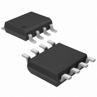
MAX3469CSA+ Maxim Integrated Products, MAX3469CSA+ Datasheet - Page 6

MAX3469CSA+
Manufacturer Part Number
MAX3469CSA+
Description
IC TXRX RS485/422 8-SOIC
Manufacturer
Maxim Integrated Products
Type
Transceiverr
Datasheet
1.MAX3468CSA.pdf
(13 pages)
Specifications of MAX3469CSA+
Number Of Drivers/receivers
1/1
Protocol
RS422, RS485
Voltage - Supply
4.75 V ~ 5.25 V
Mounting Type
Surface Mount
Package / Case
8-SOIC (3.9mm Width)
Data Rate
40 Mbps
Propagation Delay Time Ns
15 ns, 20 ns
Operating Supply Voltage
5 V
Supply Current
2.5 mA
Operating Temperature Range
0 C to + 70 C
Input Voltage
0.8 V to 2 V
Maximum Power Dissipation
471 mW
Mounting Style
SMD/SMT
Output Current
125 uA
Output Voltage
3 V
Product
RS-422/RS-485 Combination
Lead Free Status / RoHS Status
Lead free / RoHS Compliant
+5V, Fail-Safe, 40Mbps, Profibus RS-485/
RS-422 Transceivers
6
(V
MAX3465/
MAX3466
CC
_______________________________________________________________________________________
R
6, 7
10
11
12
13
14
DIFF
—
—
= +5V, T
1
2
3
4
5
8
9
FULL DUPLEX
= 54Ω
DRIVER AND RECEIVER
PROPAGATION DELAYS
A
MAX3467
= +25°C, unless otherwise noted.)
10ns/div
PIN
—
—
—
—
—
—
—
2
3
4
5
6
7
8
1
DATA RATE = 20Mbps
MAX3465 toc13
MAX3468/
MAX3469
DUPLEX
HALF
—
—
—
—
—
—
—
1
2
3
4
5
8
7
6
DI
Y, Z
RO
5V/div
2V/div
5V/div
NAME
SHDN
GND
RXP
V
TXP
RO
DE
RE
DI
Y
Z
B
A
CC
B
A
Typical Operating Characteristics (continued)
R
DIFF
Shutdown. Drive SHDN high to enter low-power shutdown mode.
Receiver Output. When RE is low and (A - B) ≥ -50mV, RO is high; if (A - B) ≤
-200mV, RO is low.
Receiver Output Enable. Drive RE low to enable RO; RO is high impedance
when RE is high. Drive RE high and DE low to enter low-power shutdown mode.
Driver Output Enable. Drive DE high to enable driver output. The driver
outputs are high impedance when DE is low. Drive RE high and DE low to
enter low-power shutdown mode. Do not leave RE unconnected when using
the MAX3466 or MAX3469.
Driver Input. With DE high, a low on DI forces the noninverting output low and
the inverting output high. Similarly, a high on DI forces the noninverting output
high and the inverting output low.
Ground
Transmitter Phase. Connect TXP to GND, or leave unconnected for normal
transmitter phase/polarity. Connect TXP to V
phase/polarity. TXP has an internal 15µA pulldown.
Noninverting Driver Output
Inverting Driver Output
Inverting Receiver Input
Noninverting Receiver Input
Receiver Phase. Connect RXP to GND, or leave unconnected for normal
receiver phase/polarity. Connect RXP to V
phase/polarity. RXP has an internal 15µA pulldown.
P osi ti ve S up p l y: + 4.75V ≤ V
Inverting Receiver Input and Inverting Driver Output
Noninverting Receiver Input and Noninverting Driver Output
= 54Ω
ENABLE RESPONSE TIME
20ns/div
MAX3465 toc14
C C
≤ + 5.25V . Byp ass V
5V/div
DE
Y, Z
1V/div
FUNCTION
R
CC
DIFF
CC
to invert the receiver
= 54Ω
C C
to invert the transmitter
to GN D w i th a 0.1µF cap acitor .
EYE DIAGRAM
Pin Description
10ns/div
DATA RATE = 20Mbps
MAX3465 toc15
Y, Z
1V/div


