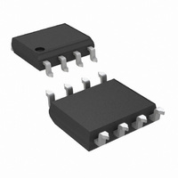
DS36276M/NOPB National Semiconductor, DS36276M/NOPB Datasheet - Page 2

DS36276M/NOPB
Manufacturer Part Number
DS36276M/NOPB
Description
IC TRANSCEIVER MUTLIPOINT 8-SOIC
Manufacturer
National Semiconductor
Type
Transceiverr
Datasheet
1.DS36276MNOPB.pdf
(12 pages)
Specifications of DS36276M/NOPB
Number Of Drivers/receivers
1/1
Protocol
RS422, RS485
Voltage - Supply
4.75 V ~ 5.25 V
Mounting Type
Surface Mount
Package / Case
8-SOIC (3.9mm Width)
Data Rate
10Mbps
Number Of Receivers
1
Number Of Transmitters
1
Number Of Transceivers
1
Data Transmission Topology
Multidrop/Multipoint
Receiver Signal Type
Differential
Transmitter Signal Type
Differential
Single Supply Voltage (typ)
5V
Single Supply Voltage (min)
4.75V
Single Supply Voltage (max)
5.25V
Dual Supply Voltage (typ)
Not RequiredV
Dual Supply Voltage (min)
Not RequiredV
Dual Supply Voltage (max)
Not RequiredV
Supply Current
60mA
Power Supply Requirement
Single
Operating Temp Range
0C to 70C
Operating Temperature Classification
Commercial
Mounting
Surface Mount
Pin Count
8
Package Type
SOIC N
Logic Case Style
SOIC
No. Of Pins
8
Operating Temperature Range
0°C To +70°C
Msl
MSL 1 - Unlimited
Termination Type
SMD
Transceiver Type
Multipoint
Driver Case Style
SOIC
Rohs Compliant
Yes
Filter Terminals
SMD
Data Rate Max
10Mbps
Supply Voltage Range
4.75V To 5.25V
Lead Free Status / RoHS Status
Lead free / RoHS Compliant
Other names
*DS36276M
*DS36276M/NOPB
DS36276M
*DS36276M/NOPB
DS36276M
www.national.com
DRIVER CHARACTERISTICS
V
V
V
V
V
I
RECEIVER CHARACTERISTICS
V
V
V
I
I
I
V
V
R
Symbol
OSD
IN
OSR
OZ
Over recommended Supply Voltage and Operating Temperature ranges, unless otherwise specified.
Electrical Characteristics
OD
oDO
oDO
T1
V
OS
V
TH
TL
HST
OH
OL
Absolute Maximum Ratings
If Military/Aerospace specified devices are required,
please contact the National Semiconductor Sales Office/
Distributors for availability and specifications.
Supply Voltage (V
Input Voltage (DE, RE , and DI)
Driver Output Voltage/
Receiver Output Voltage (RO)
Maximum Package Power Dissipation
+25˚C)
Storage Temperature Range
IN
T1
OS
Receiver Input Voltage
M Package
(derate 5.8 mW/˚C above
Differential Output Voltage
Output Voltage
Output Voltage
Differential Output Voltage
(Termination Load)
Balance of V
|V
Driver Common Mode
Output Voltage
Balance of V
|V
Driver Short-Circuit
Output Current
Differential Input High
Threshold Voltage (Note 5)
Differential Input Low
Threshold Voltage (Note 5)
Hysteresis (Note 6)
Line Input Current
(V
Short Circuit Current
TRI-STATE
Output High Voltage
( Figure 12 )
Output Low Voltage
( Figure 12 )
Input Resistance
T1
OS
CC
| − |V
| − |V
= 4.75V, 5.25V, 0V)
CC
T1
)
OS
Parameter
®
|
T1
OS
|
Leakage Current
@
+25˚C
−65˚C to +150˚C
(Notes 2, 4)
−10V to +15V
I
I
R
R
R
R
R
R
R
R
V
V
V
V
V
−7V
V
−7V
V
Other Input = 0V
DE = V
V
V
V
V
V
V
O
O
(Note 1)
O
O
O
O
O
O
CM
O
O
ID
ID
ID
ID
L
L
L
L
L
L
L
L
= 0 mA (No Load)
= 0 mA (Output to GND)
= 54
= 100
= 54
= 100
= 54
= 100
= 54
= 100
= +12V
= V
= 0V
= −7V
= V
= V
= 0V
= 0.4 to 2.4V
= 0V, I
= OPEN, I
= −0.5V, I
= −0.5V, I
= 0V
726 mW
V
V
CC
OH
OL
IH
CM
CM
5.5V
5.5V
, I
, I
(Note 7)
(485)
7V
OH
O
(422)
O
= 8.0 mA
+12V
+12V
= −0.4 mA
OL
OL
= −0.4 mA
OH
Conditions
2
= +8 mA
= +16 mA
= −0.4 mA
Lead Temperature (Soldering 4
sec.)
Max Junction Temperature
ESD Rating (HBM, 1.5 k , 100
pF)
Recommended Operating
Conditions
Supply Voltage, V
Bus Voltage
Operating Temperature (T
( Figure 1 )
(Note 3)
( Figure 1 )
(Note 3)
( Figure 3 )
V
V
DS36276
I
I
= +12V
= −7V
RO
CC
−0.2
−0.2
−0.2
−0.2
−0.5
−5.0
Min
−20
1.5
1.5
2.0
2.5
2.5
12
0
0
0
0
A
)
−0.18
−0.23
−140
−180
0.07
0.07
0.08
0.08
−0.5
0.25
0.35
Typ
134
140
−30
4.8
2.0
2.3
2.5
2.3
0.7
3.5
3.5
50
19
4.75
Min
−7
0
−290
Max
+0.2
+0.2
+0.2
+0.2
−0.8
290
−85
+20
6.0
6.0
6.0
5.0
5.0
3.0
3.0
1.0
0.6
0.7
Max
5.25
+12
+70
0
6.0 kV
260˚C
150˚C
Units
Units
mA
mA
mA
mA
mV
mA
mA
mA
µA
k
˚C
V
V
V
V
V
V
V
V
V
V
V
V
V
V
V
V
V
V
V


