DS36C278TM/NOPB National Semiconductor, DS36C278TM/NOPB Datasheet
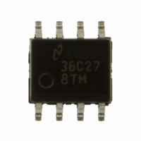
IC TRANSCEIVER EIA LP 8-SOIC

DS36C278TM/NOPB

Manufacturer Part Number
DS36C278TM/NOPB
Description
IC TRANSCEIVER EIA LP 8-SOIC
Manufacturer
National Semiconductor
Type
Transceiverr
Datasheet

Specifications of DS36C278TM/NOPB

Number Of Drivers/receivers
1/1
Protocol
RS485
Voltage - Supply
4.75 V ~ 5.25 V
Mounting Type
Surface Mount
Package / Case
8-SOIC (3.9mm Width)
Number Of Receivers
1
Number Of Transmitters
1
Number Of Transceivers
1
Data Transmission Topology
Multipoint
Receiver Signal Type
Differential
Transmitter Signal Type
Differential
Single Supply Voltage (typ)
5V
Single Supply Voltage (min)
4.75V
Single Supply Voltage (max)
5.25V
Dual Supply Voltage (typ)
Not RequiredV
Dual Supply Voltage (min)
Not RequiredV
Dual Supply Voltage (max)
Not RequiredV
Supply Current
0.5mA
Power Supply Requirement
Single
Operating Temp Range
-40C to 85C
Operating Temperature Classification
Industrial
Mounting
Surface Mount
Pin Count
8
Package Type
SOIC N
Lead Free Status / RoHS Status
Lead free / RoHS Compliant
Other names
*DS36C278TM
*DS36C278TM/NOPB
DS36C278TM

Available stocks

Company
Part Number
Manufacturer
Quantity
Price
Part Number:
DS36C278TM/NOPB
Manufacturer:
NS
Quantity:
1 524
© 2004 National Semiconductor Corporation
DS36C278
Low Power Multipoint EIA-RS-485 Transceiver
General Description
The DS36C278 is a low power differential bus/line trans-
ceiver designed to meet the requirements of RS-485 stan-
dard for multipoint data transmission. In addition it is com-
patible with TIA/EIA-422-B.
The CMOS design offers significant power savings over its
bipolar and ALS counterparts without sacrificing ruggedness
against ESD damage. The device is ideal for use in battery
powered or power conscious applications. I
500 µA maximum.
The driver and receiver outputs feature TRI-STATE
bility. The driver outputs operate over the entire common
mode range of −7V to +12V. Bus contention or fault situa-
tions that cause excessive power dissipation within the de-
vice are handled by a thermal shutdown circuit, which forces
the driver outputs into the high impedance state.
The receiver incorporates a fail safe circuit which guarantees
a high output state when the inputs are left open. (Note 1)
The DS36C278T is fully specified over the industrial tem-
perature range (−40˚C to +85˚C).
Connection Diagram
Truth Table
Note 1: Non-terminated, open input only
TRI-STATE
®
is a registered trademark of National Semiconductor Corporation.
DRIVER SECTION
RECEIVER SECTION
RE*
RE*
H
X
X
X
L
L
L
Order Number DS36C278TM, DS36C278TN,
DS012040
See NS Package Number M08A or N08E
DE
DE
H
H
L
L
L
L
L
CC
is specified at
DS36C278M, DS36C278N
DI
OPEN (Note 1)
H
X
L
®
capa-
≥+0.2V
≤−0.2V
RI-RI*
X
DO/RI
H
L
Z
Features
n 100% RS-485 compliant
n Low power CMOS design:
n Built-in power up/down glitch-free circuitry
n DIP and SOIC packages available
n Industrial temperature range: −40˚C to +85˚C
n On-board thermal shutdown circuitry
n Wide common mode range: −7V to +12V
n Receiver open input fail-safe (Note 1)
n
n
n ESD (human body model): ≥2 kV
n Drop in replacement for:
— Guaranteed RS-485 device interoperation
— Permits live transceiver insertion/displacement
— Prevents damage to the device in the event of
1
1
— LTC485, MAX485, DS75176, DS3695
4
2
01204001
unit load (DS36C278): ≥128 nodes
unit load (DS36C278T): ≥64 nodes
excessive power dissipation
DO*/RI*
RO
H
H
H
L
Z
L
Z
I
CC
500 µA max
www.national.com
July 1998

Related parts for DS36C278TM/NOPB

DS36C278TM/NOPB Summary of contents

Page 1

... RE Note 1: Non-terminated, open input only TRI-STATE ® registered trademark of National Semiconductor Corporation. © 2004 National Semiconductor Corporation Features n 100% RS-485 compliant — Guaranteed RS-485 device interoperation n Low power CMOS design: n Built-in power up/down glitch-free circuitry — Permits live transceiver insertion/displacement n DIP and SOIC packages available n Industrial temperature range: − ...

Page 2

... Absolute Maximum Ratings If Military/Aerospace specified devices are required, please contact the National Semiconductor Sales Office/ Distributors for availability and specifications. Supply Voltage ( Input Voltage (DE, RE*, & DI) Common Mode ( Driver Output/Receiver Input Input Voltage (DO/RI, DO*/RI*) Receiver Output Voltage Maximum Package Power Dissipation @ +25˚ ...

Page 3

Electrical Characteristics Over Supply Voltage and Operating Temperature ranges, unless otherwise specified Symbol Parameter RECEIVER CHARACTERISTICS I Input Balance Test B V High Level Output Voltage OH V Low Level Output Voltage OL I Short Circuit Current OSR I TRI-STATE ...

Page 4

Switching Characteristics Note 2: “Absolute Maximum Ratings” are those values beyond which the safety of the device cannot be guaranteed. They are not meant to imply that the devices should be operated at these limits. The table of “Electrical Characteristics” ...

Page 5

Parameter Measurement Information (Continued) FIGURE 7. TRI-STATE Test Circuit (t FIGURE 8. TRI-STATE Waveforms (t FIGURE 9. TRI-STATE Test Circuit (t FIGURE 10. TRI-STATE Waveforms (t 01204007 , t ) PZH PHZ FIGURE 11. Receiver V 01204008 , t ) ...

Page 6

Parameter Measurement Information FIGURE 15. Receiver Enable and Disable Waveforms (t FIGURE 16. Receiver Enable and Disable Waveforms (t www.national.com (Continued) FIGURE 14. Receiver TRI-STATE Test Circuit 6 01204014 01204015 , t ) PLZ PZL 01204016 , t ) PHZ ...

Page 7

Typical Application Information Pin Name No. Receiver Output: When RE (Receiver Enable) is LOW, the receiver is enabled (ON), if DO/RI ≥ DO*/RI 200 mV, RO will be HIGH. If DO/RI ≤ DO*/RI* by 200 mV, RO ...

Page 8

Unit Load (Continued) FIGURE 18. Input Current vs Input Voltage Operating Range www.national.com 01204019 8 ...

Page 9

Physical Dimensions inches (millimeters) unless otherwise noted 8-Lead (0.150" Wide) Molded Small Outline Package, JEDEC Order Number DS36C278TM, DS36C278M NS Package Number M08A 9 www.national.com ...

Page 10

... BANNED SUBSTANCE COMPLIANCE National Semiconductor certifies that the products and packing materials meet the provisions of the Customer Products Stewardship Specification (CSP-9-111C2) and the Banned Substances and Materials of Interest Specification (CSP-9-111S2) and contain no ‘‘Banned Substances’’ as defined in CSP-9-111S2. ...

Related keywords