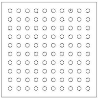
CYV15G0101DXB-BBI Cypress Semiconductor Corp, CYV15G0101DXB-BBI Datasheet - Page 26

CYV15G0101DXB-BBI
Manufacturer Part Number
CYV15G0101DXB-BBI
Description
IC TXRX HOTLINK 100-LBGA
Manufacturer
Cypress Semiconductor Corp
Series
HOTlink II™r
Type
Transceiverr
Datasheet
1.CYP15G0101DXB-BBXC.pdf
(44 pages)
Specifications of CYV15G0101DXB-BBI
Package / Case
100-LBGA
Protocol
Fibre Channel
Voltage - Supply
3.135 V ~ 3.465 V
Mounting Type
Surface Mount
Product
PHY
Supply Voltage (min)
3.135 V
Supply Current
0.51 A
Maximum Operating Temperature
+ 85 C
Minimum Operating Temperature
- 40 C
Mounting Style
SMD/SMT
Number Of Channels
1
Lead Free Status / RoHS Status
Contains lead / RoHS non-compliant
Number Of Drivers/receivers
-
Lead Free Status / RoHS Status
Lead free / RoHS Compliant, Contains lead / RoHS non-compliant
Available stocks
Company
Part Number
Manufacturer
Quantity
Price
Company:
Part Number:
CYV15G0101DXB-BBI
Manufacturer:
Cypress Semiconductor Corp
Quantity:
10 000
DC Electrical Characteristics
Over the Operating Range (continued)
AC Test Loads and Waveforms
Document Number: 38-02031 Rev. *L
Notes
I
I
V
V
V
V
V
I
I
V
30. This is the minimum difference in voltage between the true and complement inputs required to ensure detection of a logic-1 or logic-0. A logic-1 exists when
31. The common mode range defines the allowable range of INPUT+ and INPUT when INPUT+ = INPUT. This marks the zero-crossing between the true and
32. Not applicable for AC-coupled interfaces. For AC-coupled interfaces, V
33. Maximum I
34. Typical I
35. Cypress uses constant current (ATE) load configurations and forcing functions. This figure is for reference only. 5pF differential load reflects tester capacitance,
36. The LVTTL switching threshold is 1.4V. All timing references are made relative to the point where the signal edges crosses this threshold voltage.
CC
CC
IHE
ILE
Power Supply
Differential Serial Line Receiver Inputs: IN1, IN2
Parameter
OLC
ODIF
DIFFS
IHE
ILE
COM
the true (+) input is more positive than the complement () input. A logic-0 exists when the complement () input is more positive than true (+) input.
complement inputs as the signal switches between a logic-1 and a logic-0.
Driver sending a continuous alternating 01 pattern to the Serial Input Receiver.
and is recommended at low data rates only.
GND
[31, 32]
V
[30]
th
CC
= 1.4 V
1 ns
CC
is measured under similar conditions except with V
is measured with V
R1 = 590
R2 = 435
(Includes fixture and
probe capacitance)
Power supply current
REFCLK= Max
Power supply current
REFCLK = 125 MHz
C
Output LOW voltage
(V
Output differential voltage
|(OUT+) (OUT)|
Input differential voltage |(IN+) (IN)|
Highest input HIGH voltage
Lowest input LOW voltage
Input HIGH current
Input LOW current
Common mode input range
L
(c) LVTTL Input Test Waveform
(a) LVTTL Output Test Load
CC
7 pF
referenced)
2.0 V
0.8 V
CC
=
Description
3.0 V
C
MAX, with all Serial Drivers enabled, parallel outputs unloaded, sending a alternating 01 pattern to the Serial Input Receiver.
L
2.0 V
0.8 V
3.3 V
[35]
R1
R2
[36]
V
th
1 ns
CC
= 1.4 V
=
3.3V, T
DIFFS
Commercial
Industrial
Commercial
Industrial
100 differential load
150 differential load
100 differential load
150 differential load
V
V
A
IN
IN
requirement still needs to be satisfied.
=
= V
= V
25°C, parallel outputs unloaded, RXCKSEL
V
V
IHE
ILE
IHE
ILE
270 ps
Test Conditions
Min
Max
20%
(d) CML/LVPECL Input Test Waveform
(b) CML Output Test Load
R
L
= 100
80%
V
V
IHE
ILE
V
V
R
V
V
CC
Typ
=
CC
L
CYW15G0101DXB
CC
CC
80%
–700
390
390
CYP15G0101DXB
CYV15G0101DXB
Min
450
560
100
MID, and with one Serial Line
1.95 V
–
–
1.4
1.4
– 2.0
[35]
[34]
20%
V
V
Max
CC
270 ps
CC
CC
1000
1200
1350
500
510
500
510
Max
V
900
0.05
0.7
0.7
CC
–
–
[33]
Page 26 of 44
Unit
Unit
mA
mA
mA
mA
mV
mV
mV
µA
µA
V
V
V
V
V
[+] Feedback


