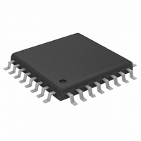
MAX9157EHJ+ Maxim Integrated Products, MAX9157EHJ+ Datasheet - Page 9

MAX9157EHJ+
Manufacturer Part Number
MAX9157EHJ+
Description
IC TXRX QUAD LVDS 32-TQFP
Manufacturer
Maxim Integrated Products
Type
Transceiverr
Datasheet
1.MAX9157EHJ.pdf
(16 pages)
Specifications of MAX9157EHJ+
Number Of Drivers/receivers
4/4
Protocol
LVDS
Voltage - Supply
3 V ~ 3.6 V
Mounting Type
Surface Mount
Package / Case
32-TQFP, 32-VQFP
Lead Free Status / RoHS Status
Lead free / RoHS Compliant
a driver located on a card in the middle of the bus is
27Ω because the driver sees two 54Ω loads in parallel.
A typical LVDS driver (rated for a 100Ω load) would not
develop a large enough differential signal to be reliably
detected by an LVDS receiver. The MAX9157 BLVDS
drivers are designed and specified to drive a 27Ω load
to differential voltage levels of 250mV to 460mV. A stan-
dard LVDS receiver is able to detect this level of differ-
ential signal. Short extensions off the bus, called stubs,
contribute to capacitive loading. Keep stubs less than
1in for a good balance between ease of component
placement and good signal integrity.
The MAX9157 driver outputs are current-source drivers
and drive larger differential signal levels into loads
lighter than 27Ω and smaller levels into loads heavier
than 27Ω (see Typical Operating Characteristics
curves). To keep loading from reducing bus impedance
below the rated 27Ω load, PC board traces can be
designed for higher unloaded characteristic impedance.
For transition times (measured from 0% to 100%) short-
er than the delay between capacitive loads, the loads
are seen as low-impedance discontinuities from which
the driven signal is reflected. Reflections add and sub-
tract from the signal being driven and cause decreased
noise margin and jitter. The MAX9157 output drivers
are designed for a minimum transition time of 1ns
(rated 0.6ns from 20% to 80%, or about 1ns from 0% to
100%) to reduce reflections while being fast enough for
high-speed backplane data transmission.
The power-on reset voltage of the MAX9157 is typically
2.25V. When the supply falls below this voltage, the
devices are disabled and the receiver inputs/driver out-
puts are in high impedance. The power-on reset
ensures glitch-free power-up and power-down, allow-
ing hot swapping of cards in a multicard bus system
without disrupting communications.
The MAX9157 receiver inputs feature 52mV hysteresis to
increase noise immunity for low-differential input signals.
The MAX9157 features driver/receiver enable inputs
that select the bus I/O function (Table 1). Tables 2 and
3 show the driver and receiver truth tables.
_______________________________________________________________________________________
Effect of Transition Times
Receiver Input Hysteresis
Operating Modes
Power-On Reset
Quad Bus LVDS Transceiver
The MAX9157 includes pullup or pulldown resistors
(300kΩ) to ensure that unconnected inputs are defined
(Table 4).
Bypass each supply pin with high-frequency surface-
mount ceramic 0.1µF and 1nF capacitors in parallel as
close to the device as possible, with the smaller value
capacitor closest to the device.
In the example given in the Effect of Capacitive Loading
section, the loaded differential impedance of a bus is
reduced to 54Ω. Since the bus can be driven from any
card position, the bus must be terminated at each end. A
parallel termination of 54Ω at each end of the bus placed
across the traces that make up the differential pair pro-
vides a proper termination. The total load seen by the dri-
ver is 27Ω. The MAX9157 drives higher differential signal
levels into lighter loads. (See Differential Output Voltage
vs. Output Load graph in the Typical Operating Char-
acteristics section). A multidrop bus with the driver at one
end and receivers connected at regular intervals along
the bus has a lowered impedance due to capacitive load-
ing. Assuming a 54Ω impedance, the multidrop bus can
be terminated with a single, parallel-connected 54Ω resis-
tor at the far end from the driver. Only a single resistor is
required because the driver sees one 54Ω differential
trace. The signal swing is larger with a 54Ω load. In gen-
eral, parallel terminate each end of the bus with a resistor
Table 1. I/O Enable Functional Table
Table 2. Driver Mode
Driver Mode
Receiver Mode
High-Impedance Mode
Loopback Mode
DE_
H
H
L
MODE SELECTED
INPUTS
DIN_
Applications Information
Input Internal Pullup/Pulldown
H
L
X
DO_+/RIN_+
H
L
Z
Supply Bypassing
DE_
OUTPUTS
H
H
L
L
Termination
Resistors
DO_-/RIN_-
RE_
H
L
Z
H
H
L
L
9


