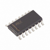
MAX4447ESE+ Maxim Integrated Products, MAX4447ESE+ Datasheet - Page 4

MAX4447ESE+
Manufacturer Part Number
MAX4447ESE+
Description
IC LDRVR SGL-DIFF 430MHZ 16-SOIC
Manufacturer
Maxim Integrated Products
Type
Line Driver, Transmitterr
Datasheet
1.MAX4447ESE.pdf
(12 pages)
Specifications of MAX4447ESE+
Number Of Drivers/receivers
1/0
Protocol
xDSL
Voltage - Supply
4.5 V ~ 5.5 V
Mounting Type
Surface Mount
Package / Case
16-SOIC (3.9mm Width)
Logic Family
MAX4447
Logic Type
Single Ended to Differential Line Drivers
Supply Voltage (max)
5.5 V
Supply Voltage (min)
4.5 V
Maximum Operating Temperature
+ 85 C
Mounting Style
SMD/SMT
Maximum Power Dissipation
1600 mW
Minimum Operating Temperature
- 40 C
Output Current
130 mA
Supply Current
46 mA
Operating Supply Voltage
5 V
Lead Free Status / RoHS Status
Lead free / RoHS Compliant
6500V/µs, Wideband, High-Output-Current, Single-
Ended-to-Differential Line Drivers with Enable
AC ELECTRICAL CHARACTERISTICS (continued)
(V
V
4
Note 1: R
Note 2: Input step voltage has <100ps rise (fall) time. Measured at the output from 10% to 90% (90% to 10%) levels.
Note 3: Includes the current noise contribution through the on-die feedback resistor.
OUT
Fall Time (Note 2)
Settling Time
Spurious-Free Dynamic Range
2nd Harmonic Distortion
3rd Harmonic Distortion
Differential Phase Error
Differential Gain Error
Input Noise Voltage Density
Input Noise Current Density
Output Impedance
Enable Time
Disable Time
Power-Up Time
Power-Down Time
CC
_______________________________________________________________________________________
= +5V, V
= V
OUT
PARAMETER
G
is the gain resistor. See Figure 1.
+ - V
EE
= -5V, R
OUT
-, T
A
L
= +25°C, unless otherwise noted.)
= 100Ω between OUT+ and OUT-, A
SYMBOL
Z
SFDR
t
t
FALL
OUT±
t
DG
DP
OFF
e
ON
i
N
N
Settle to 0.1%, V
V
V
V
V
V
V
NTSC, R
NTSC, R
f = 1MHz (Note 3)
f = 1MHz
f = 10MHz, each output to ground
V
V
V
V
OUT
OUT
OUT
OUT
OUT
OUT
IN
IN
IN
IN
= 1V, V
= 1V, V
= 1V, V
= 1V, V
= 4V step
= 8V step
= 2V step
= 2Vp-p
= 2Vp-p
= 2Vp-p
L
L
= 150Ω
= 150Ω
OUT
OUT
OUT
OUT
settle to within 1%
settle to within 1%
settle to within 1%
settle to within 1%
CONDITIONS
OUT
VCL
= 2V step
= +2V/V for MAX4447/MAX4448, A
MAX4447
MAX4448
MAX4449
MAX4447
MAX4448
MAX4449
MAX4447
MAX4448
MAX4449
f
f
f
f
f
f
f
f
f
f
f
f
C
C
C
C
C
C
C
C
C
C
C
C
= 100kHz
= 5MHz
= 20MHz
= 100MHz
= 100kHz
= 5MHz
= 20MHz
= 100MHz
= 100kHz
= 5MHz
= 20MHz
= 100MHz
MIN
VCL
1100
TYP
0.02
0.01
0.08
900
900
900
810
780
800
770
660
-78
-78
-62
-46
-78
-78
-62
-46
-86
-86
-71
-54
1.8
1.0
0.4
0.5
24
55
8
= +5V/V for MAX4449,
MAX
degrees
pA/√Hz
nV/√Hz
UNITS
dBc
dBc
dBc
ps
ns
ns
µs
µs
µs
%
Ω


