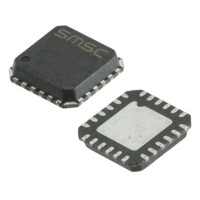
USB3316B-GJ-TR SMSC, USB3316B-GJ-TR Datasheet

USB3316B-GJ-TR
Specifications of USB3316B-GJ-TR
USB3316-GJ-TR
Available stocks
Related parts for USB3316B-GJ-TR
USB3316B-GJ-TR Summary of contents
Page 1
... Integrated ESD protection circuits ± — 15kV without any external devices SMSC USB3316 REV C USB3316 Hi-Speed USB Transceiver with 1.8V ULPI Interface - 19.2MHz Reference Clock Carkit UART mode for non-USB serial data transfers Integrated USB Switch — ...
Page 2
... Any and all such uses without prior written approval of an Officer of SMSC and further testing and/or modification will be fully at the risk of the customer. Copies of this document or other SMSC literature, as well as the Terms of Sale Agreement, may be obtained by visiting SMSC’ ...
Page 3
... The USB3316 uses SMSC’s “wrapper-less” technology to implement the ULPI interface. This “wrapper- less” technology allows the PHY to achieve a low latency transmit and receive time. SMSC’s low latency transceiver allows an existing UTMI Link to be reused by adding a UTMI to ULPI bridge. By adding a bridge to the ASIC the existing and proven UTMI Link IP can be reused ...
Page 4
... USB cable. In addition to audio signals, the switches can also be used to connect Full Speed USB from another PHY onto the USB cable. Revision 2.1 (06-10-10) Hi-Speed USB Transceiver with 1.8V ULPI Interface - 19.2MHz Reference Clock 4 PRODUCT PREVIEW SMSC USB3316 REV C ...
Page 5
... USB3316 Pin Locations and Descriptions Package Diagram with Pin Locations The pinout below is viewed from the top of the package. ID VBUS VBAT VDD3 Figure 1.1 USB3316 QFN Pinout - Top View Figure 2 USB3316 VFBGA & UFBGA Pinout - Top View SMSC USB3316 REV 24Pin QFN 3 16 4x4mm ...
Page 6
... The system must not drive voltage on the CLKOUT pin following POR or hardware reset that exceeds the value of V I/O, N/A ULPI bi-directional data bus. CMOS 6 PRODUCT PREVIEW DESCRIPTION . IH_ED SMSC USB3316 REV C ...
Page 7
... STP A3 21 VDD1 RESETB B2 23 REFCLK A2 24 RBIAS A1 FLAG GND C3 SMSC USB3316 REV C DIRECTION/ ACTIVE TYPE LEVEL I/O, N/A ULPI bi-directional data bus. CMOS I/O, N/A ULPI bi-directional data bus. CMOS I/O, N/A ULPI bi-directional data bus. DATA[0] is CMOS the LSB. ...
Page 8
... B1 ID RBIAS E3 SPKR_L E2 SPKR_R/M GND C3 Optional Switched Signal to DP/DM 8 PRODUCT PREVIEW Link Controller D3 DATA7 E4 DATA6 D4 DATA5 E5 DATA4 C4 DATA3 C5 DATA2 B4 DATA1 B5 DATA0 A3 STP A5 NXT A4 DIR D5 CLKOUT B2 RESETB A2 Reference Signal at REFCLK must comply with V and 1.8V Supply B3 C BYP A1 8.06k SMSC USB3316 REV C ...
Page 9
... VBUS installed on this side VBUS USB C Receptacle 1 VBUS GND SHIELD Figure 3.1 USB3316 QFN Application Diagram (Host or OTG) SMSC USB3316 REV C Voltage at the VBUS pin must not be allowed to exceed V . VMAX USB331X DATA7 DATA6 DATA5 DATA4 R VBUS DATA3 2 VBUS DATA2 DATA1 DATA0 ...
Page 10
... RBIAS E3 SPKR_L E2 SPKR_R/M GND C3 Optional Switched Signal to DP/DM 10 PRODUCT PREVIEW Link Controller CPEN D3 DATA7 E4 DATA6 D4 DATA5 E5 DATA4 C4 DATA3 C5 DATA2 B4 DATA1 B5 DATA0 A3 STP A5 NXT A4 DIR D5 CLKOUT B2 RESETB A2 Reference Signal at REFCLK must comply with V and 1.8V Supply B3 C BYP A1 8.06k SMSC USB3316 REV C ...
Page 11
Package Outline Figure 4.1 24-pin QFN, 4x4mm Body, 0.5mm Pitch ...
Page 12
Figure 5 25-Pin VFBGA, 3x3mm Body, 0.5mm Pitch ...
Page 13
Figure 6 25-Pin UFBGA, 3x3mm Body, 0.5mm Pitch ...


