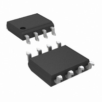
CLC007BM/NOPB National Semiconductor, CLC007BM/NOPB Datasheet - Page 3

CLC007BM/NOPB
Manufacturer Part Number
CLC007BM/NOPB
Description
IC CABLE DRIVER SERIAL 8SOIC
Manufacturer
National Semiconductor
Series
CLCr
Type
Driverr
Datasheet
1.CLC007BMNOPB.pdf
(10 pages)
Specifications of CLC007BM/NOPB
Number Of Drivers/receivers
1/0
Voltage - Supply
4.5 V ~ 5.5 V
Mounting Type
Surface Mount
Package / Case
8-SOIC (3.9mm Width)
Device Type
Line
Propagation Delay
1ns
Supply Voltage Range
4.5V To 5.5V
Driver Case Style
SOIC
No. Of Pins
8
Operating Temperature Range
-40°C To +85°C
Svhc
No SVHC (15-Dec-2010)
Rohs Compliant
Yes
Base Number
7
Number Of Channels Per Chip
1
Supply Voltage (max)
5.5 V
Supply Voltage (min)
4.5 V
Maximum Operating Temperature
+ 85 C
Mounting Style
SMD/SMT
Operating Current
39 mA
Operating Voltage
5 V
For Use With
SD007EVK - BOARD EVALUATION CLC007
Lead Free Status / RoHS Status
Lead free / RoHS Compliant
Protocol
-
Lead Free Status / Rohs Status
Details
Other names
CLC007BM
Available stocks
Company
Part Number
Manufacturer
Quantity
Price
Part Number:
CLC007BM/NOPB
Manufacturer:
TI/德州仪器
Quantity:
20 000
STATIC PERFORMANCE
Supply Current, Loaded
Supply Current, Unloaded
Output HIGH Voltage (V
Output Low Voltage (V
Input Bias Current
Output Swing
Common Mode Input Range Upper Limit
Common Mode Input Range Lower Limit
Minimum Differential Input Swing
Power Supply Rejection Ratio (Note 3)
AC PERFORMANCE
Output Rise and Fall Time
Overshoot
Propagation Delay
Duty Cycle Distortion
Residual Jitter
MISCELLANEOUS PERFORMANCE
Input Capacitance
Output Resistance
Output Inductance
Absolute Maximum Ratings
If Military/Aerospace specified devices are required,
please contact the National Semiconductor Sales Office/
Distributors for availability and specifications.
Electrical Characteristics
(V
Note 1: “Absolute Maximum Ratings” are those values beyond which the safety of the device cannot be guaranteed. They are not meant to imply that the devices
should be operated at these limits. The table of “Electrical Characteristics” specifies conditions of device operation.
Note 2: Min/max ratings are based on product characterization and simulation. Individual parameters are tested as noted. Outgoing quality levels are determined
from tested parameters.
Note 3: Spec is 100% tested at +25°C
Note 4: Measured between the 20% and 80% levels of the waveform.
Note 5: Measured with both outputs driving 150Ω, AC coupled at 270 Mbps.
Supply Voltage
Output Current
Maximum Junction Temperature
Storage Temperature Range
Lead Temperature
ESD Rating (Human body Model)
CC
(Soldering 10 Second)
= 0V, V
Parameter
EE
= −5V; unless otherwise specified).
OL
OH
)
)
(Note 5)
(Note 3)
(Note 3)
(Note 3)
(Note 3)
(Notes 3, 4, 5)
−65°C to +150°C
Conditions
(Note 1)
+125°C
+300°C
30 mA
1000V
6V
3
Typ +25°C
Recommended Operating
Conditions
Package Thermal Resistance
θ
θ
Reliability Information
Supply Voltage (V
MTTF
−1.7
−3.3
1.65
−0.7
−2.6
200
650
1.0
1.0
39
34
10
26
50
25
10
JA
JC
5
6
8–pin SOIC
8–pin SOIC
1.55/1.75
Min/Max
−2.0/1.4
−3.6/3.0
425/955
+25°C
28/45
−0.8
−2.5
200
30
20
—
—
CC
– V
EE
)
1.53/1.77
400/1100
Min/Max
−2.0/1.4
−3.6/3.0
0°C to
+70°C
26/47
−0.8
−2.5
200
50
20
—
—
1.51/1.79
400/1100
Min/Max
−40°C to
−2.0/1.4
−3.6/3.0
+85°C
26/47
−0.8
−2.5
200
50
20
—
—
+4.5V to +5.5V
www.national.com
+105°C/W
254 Mhr
+160°C
Units
ps
mA
mA
mV
nH
μA
dB
pF
ps
ns
ps
%
Ω
V
V
V
V
V
pp


