DS90CF366MTD/NOPB National Semiconductor, DS90CF366MTD/NOPB Datasheet - Page 2
DS90CF366MTD/NOPB
Manufacturer Part Number
DS90CF366MTD/NOPB
Description
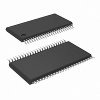
IC RCVR LVDS FPD 18BIT 48-TSSOP
Manufacturer
National Semiconductor
Type
Receiverr
Datasheet
1.DS90CF386MTDNOPB.pdf
(18 pages)
Specifications of DS90CF366MTD/NOPB
Number Of Drivers/receivers
0/1
Protocol
RS644
Voltage - Supply
3 V ~ 3.6 V
Mounting Type
Surface Mount
Package / Case
48-TSSOP
Supply Current
135mA
Driver Case Style
TSSOP
No. Of Pins
48
Operating Temperature Range
-10°C To +70°C
Msl
MSL 2 - 1 Year
Supply Voltage Min
3V
Peak Reflow Compatible (260 C)
Yes
No. Of Receivers
3
Rohs Compliant
Yes
Interface Type
LVDS/Serial/SPI
Leaded Process Compatible
Yes
Lead Free Status / RoHS Status
Lead free / RoHS Compliant
Other names
*DS90CF366MTD
*DS90CF366MTD/NOPB
DS90CF366MTD
*DS90CF366MTD/NOPB
DS90CF366MTD
Available stocks
Company
Part Number
Manufacturer
Quantity
Price
Company:

Part Number:
DS90CF366MTD/NOPB
Manufacturer:
NS
Quantity:
488


www.national.com
CMOS/TTL DC SPECIFICATIONS
V
V
V
V
V
I
I
LVDS RECEIVER DC SPECIFICATIONS
V
V
I
RECEIVER SUPPLY CURRENT
ICCRW
ICCRW
ICCRG
IN
OS
Symbol
IN
IH
IL
OH
OL
CL
TH
TL
Absolute Maximum Ratings
If Military/Aerospace specified devices are required,
please contact the National Semiconductor Sales Office/
Distributors for availability and specifications.
Supply Voltage (V
CMOS/TTL Output Voltage
LVDS Receiver Input Voltage
Junction Temperature
Storage Temperature
Lead Temperature
Solder Reflow Temperature
Maximum Package Power
Dissipation Capacity @ 25°C
Package Derating:
Electrical Characteristics
Over recommended operating supply and temperature ranges unless otherwise specified.
TSSOP)
MTD56 (TSSOP) Package:
MTD48 (TSSOP) Package:
DS90CF386MTD
(Soldering, 4 sec for
(Soldering, 20 sec for FBGA)
DS90CF386MTD
DS90CF366MTD
High Level Input Voltage
Low Level Input Voltage
High Level Output Voltage
Low Level Output Voltage
Input Clamp Voltage
Input Current
Output Short Circuit Current
Differential Input High Threshold
Differential Input Low Threshold
Input Current
Receiver Supply Current
Worst Case
Receiver Supply Current
Worst Case
Receiver Supply Current,
16 Grayscale
CC
)
Parameter
12.4 mW/°C above +25°C
−0.3V to (V
−0.3V to (V
−65°C to +150°C
−0.3V to +4V
(Note
CC
CC
I
I
I
V
V
V
V
V
V
C
Worst Case Pattern,
DS90CF386 (Figures 1,
4 )
C
Worst Case Pattern,
DS90CF366 (Figures 1,
4 )
C
16 Grayscale Pattern,
OH
OL
CL
+150°C
+260°C
+220°C
+ 0.3V)
+ 0.3V)
1.61 W
1.89 W
IN
IN
OUT
L
L
L
1)
CM
IN
IN
= 8 pF,
= 8 pF,
= 8 pF,
= 2 mA
= −18 mA
= - 0.4 mA
= 0.4V, 2.5V or V
= GND
= +2.4V, V
= 0V, V
= +1.2V
= 0V
CC
2
= 3.6V
CC
Maximum Package Power
Dissipation Capacity @ 25°C
Package Derating:
ESD Rating
Recommended Operating
Conditions
Conditions
= 3.6V
DS90CF366MTD
SLC64A Package:
DS90CF386SLC
(HBM, 1.5 kΩ, 100 pF)
Supply Voltage (V
Operating Free Air
Receiver Input Range
Supply Noise Voltage (V
DS90CF386SLC
(EIAJ, 0Ω, 200 pF)
CC
Temperature (T
f = 32.5 MHz
f = 37.5 MHz
f = 65 MHz
f = 85 MHz
f = 32.5 MHz
f = 37.5 MHz
f = 65 MHz
f = 85 MHz
f = 32.5 MHz
f = 37.5 MHz
CC
A
)
)
CC
)
GND
−100
Min
2.0
2.7
-10
Min
−10 +25 +70
3.0
10.2 mW/°C above +25°C
0
15 mW/°C above +25°C
-0.79
0.06
+1.8
Typ
3.3
No
3.3
-60
m
49
53
81
96
49
53
78
90
28
30
0
Max Units
100
3.6
2.4
+100
VCC
-120
Max
-1.5
+15
±10
±10
114
135
100
115
0.8
0.3
70
75
60
65
45
47
mV
°C
> 700V
V
V
> 7 kV
2.0 W
PP
Units
mA
mV
mV
mA
mA
mA
mA
mA
mA
mA
mA
mA
mA
uA
uA
μA
μA
V
V
V
V
V
Related parts for DS90CF366MTD/NOPB
Image
Part Number
Description
Manufacturer
Datasheet
Request
R

Part Number:
Description:
National Semiconductor [8-Bit D/A Converter]
Manufacturer:
National Semiconductor
Datasheet:
Part Number:
Description:
National Semiconductor [Media Coprocessor]
Manufacturer:
National Semiconductor
Datasheet:
Part Number:
Description:
Digitally Controlled Tone and Volume Circuit with Stereo Audio Power Amplifier, Microphone Preamp Stage and National 3D Sound
Manufacturer:
National Semiconductor
Datasheet:
Part Number:
Description:
Digitally Controlled Tone and Volume Circuit with Stereo Audio Power Amplifier, Microphone Preamp Stage and National 3D Sound
Manufacturer:
National Semiconductor
Datasheet:
Part Number:
Description:
AC97 Rev 2 Codec with Sample Rate Conversion and National 3D Sound
Manufacturer:
National Semiconductor
Part Number:
Description:
Manufacturer:
National Semiconductor
Datasheet:
Part Number:
Description:
Manufacturer:
National Semiconductor
Datasheet:
Part Number:
Description:
General Purpose, Low Voltage, Low Power, Rail-to-Rail Output Operational Amplifiers
Manufacturer:
National Semiconductor
Datasheet:
Part Number:
Description:
8-bit 20 MSPS flash A/D converter.
Manufacturer:
National Semiconductor
Datasheet:
Part Number:
Description:
Low Noise Quad Operational Amplifier
Manufacturer:
National Semiconductor
Datasheet:
Part Number:
Description:
Quad Differential Line Receivers
Manufacturer:
National Semiconductor
Datasheet:
Part Number:
Description:
Quad High Speed Trapezoidal? Bus Transceiver
Manufacturer:
National Semiconductor
Datasheet:
Part Number:
Description:
Dual Line Receiver
Manufacturer:
National Semiconductor
Datasheet:
Part Number:
Description:
TTL to 10k ECL Level Translator with Latch
Manufacturer:
National Semiconductor
Datasheet: