DS92CK16TMTC/NOPB National Semiconductor, DS92CK16TMTC/NOPB Datasheet - Page 5
DS92CK16TMTC/NOPB
Manufacturer Part Number
DS92CK16TMTC/NOPB
Description
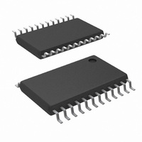
IC TRANSCEIVER 3V BLVDS 24-TSSOP
Manufacturer
National Semiconductor
Type
Transceiverr
Datasheet
1.DS92CK16TMTCNOPB.pdf
(12 pages)
Specifications of DS92CK16TMTC/NOPB
Number Of Drivers/receivers
1/1
Protocol
LVDS
Voltage - Supply
3 V ~ 3.6 V
Mounting Type
Surface Mount
Package / Case
24-TSSOP
Number Of Transmitters
1
Power Supply Requirement
Single
Package Type
TSSOP
Operating Temperature Classification
Industrial
Mounting
Surface Mount
Operating Temperature (max)
85C
Operating Temperature (min)
-40C
Supply Current
25mA
Dual Supply Voltage (typ)
Not RequiredV
Dual Supply Voltage (max)
Not RequiredV
Dual Supply Voltage (min)
Not RequiredV
Lead Free Status / RoHS Status
Lead free / RoHS Compliant
Other names
*DS92CK16TMTC
*DS92CK16TMTC/NOPB
DS92CK16TMTC
*DS92CK16TMTC/NOPB
DS92CK16TMTC
Available stocks
Company
Part Number
Manufacturer
Quantity
Price
Company:

Part Number:
DS92CK16TMTC/NOPB
Manufacturer:
National Semiconductor
Quantity:
135


DIFFERENTIAL RECEIVER CHARACTERISTICS
t
t
t
t
t
t
t
t
t
f
DIFFERENTIAL DRIVER TIMING REQUIREMENTS
t
t
t
t
t
t
t
t
t
t
t
t
f
PHLDR
PLHDR
SK1R
SK2R
SK3R
TLHR
THLR
PLHOER
PHLOER
MAX
PHLDD
PLHDD
PHLCrd
PLHCrd
SK1D
SK2D
TLHD
THLD
PHZD
PLZD
PZHD
PZLD
MAX
Symbol
Switching Characteristics
Over Supply Voltage and Operating Temperature ranges, unless otherwise specified (Notes 7, 8).
Note 1: “Absolute Maximum Ratings” are those values beyond which the safety of the device cannot be guaranteed. These ratings are not meant to imply that the
devices should be operated at these limits. The table of “Electrical Characteristics” specifies conditions of device operation.
Note 2: ESD Rating: ESD qualification is performed per the following: HBM (1.5 kΩ, 100 pF), Machine Model (250V, 0Ω), IEC 1000-4-2. All VCC pins connected
together, all ground pins connected together.
Note 3: Current into device pins is defined as positive. Current out of device pins is defined as negative. All voltages are referenced to ground except VID, VOD,
VTH, and VTL.
Note 4: All typicals are given for: V
Note 5: The VCMR range is reduced for larger VID. Example: If VID=400 mV, then VCMR is 0.2V to 2.2V A VID up to |V
CLKI/O+ and CLKI/O− inputs, with the Common Mode set to V
Note 6: Only one output should be momentarily shorted at a time. Do not exceed package power dissipation rating.
Note 7: C
Note 8: Generator waveform for all tests unless otherwise specified: f = 25 MHz, Zo = 50Ω, t
minimum skew, clock input edge rates should not be slower than 1 ns/V; control signals not slower than 3 ns/V. In general, the faster the input edge rate, the better
the AC performance.
Note 9: All device output transition times are based on characterization measurements and are guaranteed by design.
L
includes probe and fixture capacitance.
Differential Propagation Delay High to Low. CLKI/O to
CLK
Differential Propagation Delay Low to High. CLKI/O to
CLK
Duty Cycle Distortion(Note 10)
(pulse skew)
|t
Channel to Channel Skew; Same Edge (Note 11)
Part to Part Skew (Note 12)
Transition Time Low to High (Note 9)
(20% to 80% )
Transition Time High to Low(Note 9)
(80% to 20% )
Propagation Delay Low to High
( OEto CLK
Propagation Delay High to Low
(OE to CLK
Maximum Operating Frequency (Note 15)
Differential Propagation Delay High to Low. CrdCLK
CLKI/O
Differential Propagation Delay Low to High. CrdCLK
CLKI/O
CrdCLK
CrdCLK
Duty Cycle Distortion (pulse skew)
|t
Differential Part-to-Part Skew (Note 14)
Differential Transition Time (Note 9)
(20% to 80% )
Differential Transition Time (Note 9)
(80% to 20% )
Transition Time High to TRI-STATE. DE to CLKI/O
Transition Time Low to TRI-STATE. DE to CLKI/O
Transition Time TRI-STATE to High. DE to CLKI/O
Transition Time TRI-STATE to Low. DE to CLKI/O
Maximum Operating Frequency (Note 15)
PLH
PLH
OUT
OUT
–t
–t
PHL
PHL
IN
IN
|
| (Note 13)
to CLK
to CLK
OUT
OUT
)
)
OUT
OUT
CC
= +3.3V and T
Propagation Delay High to Low
Propagation Delay Low to High
Parameter
A
= +25˚C.
CC
/2.
IN
IN
5
to
to
C
VID = 250 mV
Figures 1, 2
C
Figures 3, 4
C
R
Figures 6, 7
C
Figures 8, 9
V
C
R
Figures 10, 11
IN
L
L
L
L
L
L
L
r
= 15 pF
= 15 pF
= 15 pF
= 37.5Ω
= 15 pF
= 15 pF,
= 37.5Ω
= 1 ns, t
= 0V to V
Conditions
f
= 1 ns (10%–90%). To ensure fastest propagation delay and
CC
Min
100
100
1.3
1.3
0.4
0.4
1.0
1.0
0.5
0.5
2.0
2.0
0.4
0.4
CC
–0V| may be applied between the
0.75
0.75
Typ
100
125
125
2.8
2.9
1.4
1.3
1.8
1.8
4.5
4.5
30
3
3
Max
400
600
3.8
3.8
2.5
2.4
2.2
4.5
4.5
2.5
2.5
6.0
6.0
2.0
1.4
1.4
80
10
10
32
32
www.national.com
Units
MHz
MHz
ns
ns
ps
ps
ns
ns
ns
ns
ns
ns
ns
ns
ns
ps
ns
ns
ns
ns
ns
ns
ns
Related parts for DS92CK16TMTC/NOPB
Image
Part Number
Description
Manufacturer
Datasheet
Request
R

Part Number:
Description:
National Semiconductor [8-Bit D/A Converter]
Manufacturer:
National Semiconductor
Datasheet:
Part Number:
Description:
National Semiconductor [Media Coprocessor]
Manufacturer:
National Semiconductor
Datasheet:
Part Number:
Description:
Digitally Controlled Tone and Volume Circuit with Stereo Audio Power Amplifier, Microphone Preamp Stage and National 3D Sound
Manufacturer:
National Semiconductor
Datasheet:
Part Number:
Description:
Digitally Controlled Tone and Volume Circuit with Stereo Audio Power Amplifier, Microphone Preamp Stage and National 3D Sound
Manufacturer:
National Semiconductor
Datasheet:
Part Number:
Description:
AC97 Rev 2 Codec with Sample Rate Conversion and National 3D Sound
Manufacturer:
National Semiconductor
Part Number:
Description:
Manufacturer:
National Semiconductor
Datasheet:
Part Number:
Description:
Manufacturer:
National Semiconductor
Datasheet:
Part Number:
Description:
General Purpose, Low Voltage, Low Power, Rail-to-Rail Output Operational Amplifiers
Manufacturer:
National Semiconductor
Datasheet:
Part Number:
Description:
8-bit 20 MSPS flash A/D converter.
Manufacturer:
National Semiconductor
Datasheet:
Part Number:
Description:
Low Noise Quad Operational Amplifier
Manufacturer:
National Semiconductor
Datasheet:
Part Number:
Description:
Quad Differential Line Receivers
Manufacturer:
National Semiconductor
Datasheet:
Part Number:
Description:
Quad High Speed Trapezoidal? Bus Transceiver
Manufacturer:
National Semiconductor
Datasheet:
Part Number:
Description:
Dual Line Receiver
Manufacturer:
National Semiconductor
Datasheet:
Part Number:
Description:
TTL to 10k ECL Level Translator with Latch
Manufacturer:
National Semiconductor
Datasheet: