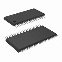
DS90CF364MTD/NOPB National Semiconductor, DS90CF364MTD/NOPB Datasheet - Page 14

DS90CF364MTD/NOPB
Manufacturer Part Number
DS90CF364MTD/NOPB
Description
IC RCVR LVDS FPD 18BIT 48-TSSOP
Manufacturer
National Semiconductor
Type
Driverr
Specifications of DS90CF364MTD/NOPB
Number Of Drivers/receivers
1/0
Protocol
RS644
Voltage - Supply
3 V ~ 3.6 V
Mounting Type
Surface Mount
Package / Case
48-TSSOP
Supply Current
105mA
Supply Voltage Range
3V To 3.6V
Driver Case Style
TSSOP
No. Of Pins
48
Operating Temperature Range
-40°C To +85°C
Msl
MSL 2 - 1 Year
Device Type
Clock
Filter Terminals
SMD
Rohs Compliant
Yes
Esd Hbm
7kV
Lead Free Status / RoHS Status
Lead free / RoHS Compliant
Other names
*DS90CF364MTD
*DS90CF364MTD/NOPB
DS90CF364MTD
*DS90CF364MTD/NOPB
DS90CF364MTD
Available stocks
Company
Part Number
Manufacturer
Quantity
Price
Company:
Part Number:
DS90CF364MTD/NOPB
Manufacturer:
Texas Instruments
Quantity:
150
www.national.com
Pin Diagrams
Truth Table
Applications Information
The DS90C363 and DS90CF364 are backward compatible
with the existing 5V FPD Link transmitter/receiver pair
(DS90CF563 and DS90CF564). To upgrade from a 5V to a
3.3V system the following must be addressed:
1.
2.
Change 5V power supply to 3.3V. Provide this supply to
the V
and receiver devices. This change may enable the
removal of a 5V supply from the system, and power may
be supplied from an existing 3V power source.
The DS90C363 (transmitter) incorporates a rise/fall
strobe select pin. This select function is on pin 14,
formerly a V
rise/fall strobe select pin is connected to V
configured with a rising edge strobe. In a system
currently using a 5V rising edge strobe transmitter
CC
, LVDS V
CC
connection on the 5V products. When the
CC
and PLL V
DS90C363
CC
R_FB
R_FB
Pin
of both the transmitter
TABLE 1. Programmable Transmitter
R_FB = V
R_FB = GND
CC
1288623
, the part is
Condition
CC
14
3.
Rising edge strobe
Falling edge strobe
(DS90CR563), no layout changes are required to
accommodate the new rise/fall select pin on the 3.3V
transmitter. The V
device will be configured with a rising edge strobe.
When converting from a 5V falling edge transmitter
(DS90CF563) to the 3V transmitter a minimal board
layout change is necessary. The 3.3V transmitter will
not be configured with a falling edge strobe if V
remains connected to the select pin. To guarantee the
3.3V transmitter functions with a falling edge strobe pin
14 should be connected to ground OR left unconnected.
When not connected (left open) and internal pull-down
resistor ties pin 14 to ground, thus configuring the
transmitter with a falling edge strobe.
The DS90C363 transmitter input and control inputs
accept 3.3V TTL/CMOS levels. They are not 5V tolerant.
Strobe Status
CC
DS90CF364
signal may remain at pin 14, and the
1288613
CC


