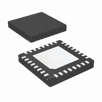
DS91M040TSQ/NOPB National Semiconductor, DS91M040TSQ/NOPB Datasheet - Page 6

DS91M040TSQ/NOPB
Manufacturer Part Number
DS91M040TSQ/NOPB
Description
IC TRANSCEIVER M-LVDS QUAD 32LLP
Manufacturer
National Semiconductor
Type
Transceiverr
Datasheet
1.DS91M040TSQNOPB.pdf
(16 pages)
Specifications of DS91M040TSQ/NOPB
Number Of Drivers/receivers
4/4
Protocol
LVDS
Voltage - Supply
3 V ~ 3.6 V
Mounting Type
Surface Mount
Package / Case
32-LLP
Device Type
Transceiver
Supply Current Max
67mA
Signaling Rate
250Mbps
Output Level Type
LVCMOS
Supply Voltage Range
3V To 3.6V
Esd Hbm
8kV
Operating Temperature Range
-40°C To +85°C
Rohs Compliant
Yes
For Use With
DS91M040EVK - BOARD EVALUATION DS91M040
Lead Free Status / RoHS Status
Lead free / RoHS Compliant
Other names
DS91M040TSQTR
Available stocks
Company
Part Number
Manufacturer
Quantity
Price
Company:
Part Number:
DS91M040TSQ/NOPB
Manufacturer:
TI
Quantity:
1 710
Part Number:
DS91M040TSQ/NOPB
Manufacturer:
TI/德州仪器
Quantity:
20 000
www.national.com
DRIVER AC SPECIFICATIONS
t
t
t
t
t
t
t
t
t
t
t
t
RECEIVER AC SPECIFICATIONS
t
t
t
t
t
t
t
t
t
t
t
t
t
GENERIC AC SPECIFICATIONS
t
f
PLH
PHL
SKD1
SKD2
SKD3
SKD4
TLH
THL
PZH
PZL
PLZ
PHZ
PLH
PHL
SKD1A
SKD1B
SKD2
SKD3
SKD4
TLH
THL
PZH
PZL
PLZ
PHZ
WKUP
MAX
Switching Characteristics
Over recommended operating supply and temperature ranges unless otherwise specified.
Note 10: The Electrical Characteristics tables list guaranteed specifications under the listed Recommended Operating Conditions except as otherwise modified
or specified by the Electrical Characteristics Conditions and/or Notes. Typical specifications are estimations only and are not guaranteed.
Note 11: Typical values represent most likely parametric norms for V
product characterization and are not guaranteed.
Note 12: Specification is guaranteed by characterization and is not tested in production.
Note 13: t
going edge of the same channel.
Note 14: t
Note 15: t
devices at the same V
Note 16: t
recommended operating temperature and voltage ranges, and across process distribution. t
Note 17: C
Note 18: Measured on a clock edge with a histogram and an acummulation of 1500 histogram hits. Input stimulus jitter is subracted geometrically.
Symbol
SKD1
SKD2
SKD3
SKD4
L
includes fixture capacitance and C
, |t
, Channel-to-Channel Skew, is the difference in propagation delay (t
, Part-to-Part Skew, is defined as the difference between the minimum and maximum differential propagation delays. This specification applies to
, Part-to-Part Skew, is the differential channel-to-channel skew of any event between devices. This specification applies to devices over
PLHD
Differential Propagation Delay Low to High
Differential Propagation Delay High to Low
Pulse Skew
Channel-to-Channel Skew
14)
Part-to-Part Skew
Part-to-Part Skew
Rise Time
Fall Time
Enable Time (Z to Active High)
Enable Time (Z to Active Low )
Disable Time (Active Low to Z)
Disable Time (Active High to Z)
Propagation Delay Low to High
Propagation Delay High to Low
Pulse Skew (Receiver Type 1)
(Note
Pulse Skew (Receiver Type 2)
(Note
Channel-to-Channel Skew
14)
Part-to-Part Skew
Part-to-Part Skew
Rise Time
Fall Time
Enable Time (Z to Active High)
Enable Time (Z to Active Low)
Disable Time (Active Low to Z)
Disable Time (Active High to Z)
Wake Up Time
(Master Device Enable (MDE) time)
Maximum Operating Frequency
− t
DD
PHLD
12,
12,
and within 5°C of each other within the operating temperature range.
|, Pulse Skew, is the magnitude difference in differential propagation delay time between the positive going edge and the negative
(Note
Note
Note
(Note
(Note
(Note
(Note
13)
13)
(Note
12)
12)
Parameter
12)
12)
(Note
(Note
(Note
(Note
12,
12)
Note
D
12,
12,
12,
16)
includes probe capacitance.
(Note
(Note
13)
Note
Note
Note
(Note
(Note
12,
12,
15)
16)
15)
Note
Note
10,
12)
Note
DD
= +3.3V and T
R
C
Figures 7, 8
R
C
Figures 9, 10
C
Figures 11, 12, 13
R
Figures 14, 15
11,
L
D
L
D
L
L
= 50Ω, C
= 50Ω, C
= 15 pF
= 500Ω, C
6
= 0.5 pF
= 0.5 pF
Note
PLHD
A
17)
or t
= +25°C, and at the Recommended Operation Conditions at the time of
L
L
PHLD
Conditions
L
SKD4
= 5 pF,
= 5 pF,
= 15 pF
) among all output channels.
is defined as |Max − Min| differential propagation delay.
Min
125
1.5
1.5
1.2
1.2
1.5
1.5
0.3
0.3
0.65
Typ
100
475
3.3
3.3
0.8
2.0
2.0
7.5
8.0
7.0
7.0
3.0
3.1
0.6
1.1
3.5
3.5
30
55
60
3
3
Max
11.5
11.5
11.5
11.5
125
200
325
800
300
500
5.5
5.5
1.6
3.0
3.0
4.5
4.5
1.2
1.6
1.6
5.5
5.5
5.5
5.5
4
3
Units
MHz
ms
ns
ns
ps
ps
ns
ns
ns
ns
ns
ns
ns
ns
ns
ns
ps
ps
ps
ns
ns
ns
ns
ns
ns
ns
ns


