DP83848TSQ/NOPB National Semiconductor, DP83848TSQ/NOPB Datasheet - Page 33
DP83848TSQ/NOPB
Manufacturer Part Number
DP83848TSQ/NOPB
Description
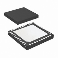
IC TXRX ETHERNET PHYTER 40-LLP
Manufacturer
National Semiconductor
Type
Transceiverr
Specifications of DP83848TSQ/NOPB
Number Of Drivers/receivers
1/1
Protocol
Ethernet
Voltage - Supply
3 V ~ 3.6 V
Mounting Type
Surface Mount
Package / Case
40-LLP
Data Rate
100Mbps
Supply Voltage Range
3V To 3.6V
Logic Case Style
LLP
No. Of Pins
40
Operating Temperature Range
-40°C To +85°C
Msl
MSL 2 - 1 Year
Filter Terminals
SMD
Rohs Compliant
Yes
Data Rate Max
10Mbps
Driver Case Style
LLP
For Use With
DP83848T-MAU-EK - BOARD EVALUATION DP83848T
Lead Free Status / RoHS Status
Lead free / RoHS Compliant
Other names
DP83848TSQTR
Available stocks
Company
Part Number
Manufacturer
Quantity
Price
Company:

Part Number:
DP83848TSQ/NOPB
Manufacturer:
TI
Quantity:
2 000
Company:
Part Number:
DP83848TSQ/NOPB
Manufacturer:
LT
Quantity:
807


5.2 ESD Protection
Typically, ESD precautions are predominantly in effect
when handling the devices or board before being installed
in a system. In those cases, strict handling procedures
need be implemented during the manufacturing process to
greatly reduce the occurrences of catastrophic ESD
events. After the system is assembled, internal compo-
nents are less sensitive from ESD events.
See Section 8.0 for ESD rating.
5.3 Clock In (X1) Recommendations
The DP83848T supports an external CMOS level oscillator
source or a crystal resonator device.
Oscillator
If an external clock source is used, X1 should be tied to the
clock source and X2 should be left floating.
The CMOS oscillator specifications for MII Mode are listed
in Table 7 25 MHz Oscillator Specification. For RMII Mode,
the CMOS oscillator specifications are listed in Table 8 50
MHz Oscillator Specification. For RMII mode, it is not rec-
ommended that the system clock out, Pin 21, be used as
the reference clock to the MAC without first verifying the
interface timing. See AN-1405 for more details.
Crystal
A 25 MHz, parallel, 20 pF load crystal resonator should be
used if a crystal source is desired. Figure 12 shows a typi-
cal connection for a crystal resonator circuit. The load
capacitor values will vary with the crystal vendors; check
with the vendor for the recommended loads.
1. This limit is provided as a guideline for component selection and not guaranteed by production testing. Refer to
AN-1548, “PHYTER 100 Base-TX Reference Clock Jitter Tolerance,” for details on jitter performance.
Rise / Fall Time
Parameter
Frequency
Frequency
Frequency
Tolerance
Symmetry
Stability
Jitter
Jitter
40%
Min
Table 7. 25 MHz Oscillator Specification
Typ
25
33
The oscillator circuit is designed to drive a parallel reso-
nance AT cut crystal with a minimum drive level of 100µW
and a maximum of 500µW. If a crystal is specified for a
lower drive level, a current limiting resistor should be
placed in series between X2 and the crystal.
As a starting point for evaluating an oscillator circuit, if the
requirements for the crystal are not known, C
should be set at 33 pF, and R
Specification for 25 MHz crystal are listed in Table 9 25
MHz Crystal Specification.
800
800
Max
60%
+50
+50
Figure 12. Crystal Oscillator Circuit
C
6
L1
1
1
X1
Units
MHz
nsec
psec
psec
ppm
ppm
1
should be set at 0 .
X2
Operational Tem-
R
www.national.com
1 year aging
C
20% - 80%
Duty Cycle
Condition
Short term
Long term
1
L2
perature
L1
and C
L2
Related parts for DP83848TSQ/NOPB
Image
Part Number
Description
Manufacturer
Datasheet
Request
R

Part Number:
Description:
BOARD EVALUATION DP83848T
Manufacturer:
National Semiconductor
Datasheet:
Part Number:
Description:
National Semiconductor [8-Bit D/A Converter]
Manufacturer:
National Semiconductor
Datasheet:
Part Number:
Description:
National Semiconductor [Media Coprocessor]
Manufacturer:
National Semiconductor
Datasheet:
Part Number:
Description:
Digitally Controlled Tone and Volume Circuit with Stereo Audio Power Amplifier, Microphone Preamp Stage and National 3D Sound
Manufacturer:
National Semiconductor
Datasheet:
Part Number:
Description:
Digitally Controlled Tone and Volume Circuit with Stereo Audio Power Amplifier, Microphone Preamp Stage and National 3D Sound
Manufacturer:
National Semiconductor
Datasheet:
Part Number:
Description:
AC97 Rev 2 Codec with Sample Rate Conversion and National 3D Sound
Manufacturer:
National Semiconductor
Part Number:
Description:
Manufacturer:
National Semiconductor
Datasheet:
Part Number:
Description:
Manufacturer:
National Semiconductor
Datasheet:
Part Number:
Description:
General Purpose, Low Voltage, Low Power, Rail-to-Rail Output Operational Amplifiers
Manufacturer:
National Semiconductor
Datasheet:
Part Number:
Description:
8-bit 20 MSPS flash A/D converter.
Manufacturer:
National Semiconductor
Datasheet:
Part Number:
Description:
Low Noise Quad Operational Amplifier
Manufacturer:
National Semiconductor
Datasheet:
Part Number:
Description:
Quad Differential Line Receivers
Manufacturer:
National Semiconductor
Datasheet:
Part Number:
Description:
Quad High Speed Trapezoidal? Bus Transceiver
Manufacturer:
National Semiconductor
Datasheet:
Part Number:
Description:
Dual Line Receiver
Manufacturer:
National Semiconductor
Datasheet: