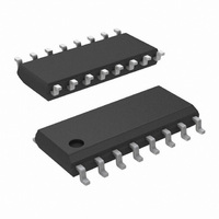
DS90C031BTM/NOPB National Semiconductor, DS90C031BTM/NOPB Datasheet - Page 2

DS90C031BTM/NOPB
Manufacturer Part Number
DS90C031BTM/NOPB
Description
IC LINE DRV LVDS QUD CMOS 16SOIC
Manufacturer
National Semiconductor
Type
Driverr
Specifications of DS90C031BTM/NOPB
Number Of Drivers/receivers
4/0
Protocol
LVDS
Voltage - Supply
4.5 V ~ 5.5 V
Mounting Type
Surface Mount
Package / Case
16-SOIC (3.9mm Width)
Number Of Drivers
4
Number Of Receivers
4
Data Rate
155.5 Mbps
Operating Supply Voltage
5 V
Maximum Power Dissipation
1068 mW
Maximum Operating Temperature
+ 85 C
Minimum Operating Temperature
- 40 C
Mounting Style
SMD/SMT
Propagation Delay Time
3 ns
Supply Voltage (max)
5.5 V
Supply Voltage (min)
4.5 V
Supply Current
21mA
Supply Voltage Range
4.5V To 5.5V
Driver Case Style
SOP
No. Of Pins
16
Operating Temperature Range
-40°C To +85°C
Msl
MSL 1 - Unlimited
Data Rate Max
155.5Mbps
Rohs Compliant
Yes
Lead Free Status / RoHS Status
Lead free / RoHS Compliant
Other names
*DS90C031BTM
DS90C031BTM
DS90C031BTM
Available stocks
Company
Part Number
Manufacturer
Quantity
Price
Company:
Part Number:
DS90C031BTM/NOPB
Manufacturer:
NS
Quantity:
2 000
www.national.com
Symbol
t
t
t
t
V
V
V
V
V
V
I
V
I
I
I
I
I
I
PHLD
PLHD
SKD
SK1
Symbol
I
OS
OZ
OFF
CC
CCL
CCZ
Absolute Maximum Ratings
If Military/Aerospace specified devices are required,
please contact the National Semiconductor Sales Office/
Distributors for availability and specifications.
Electrical Characteristics
Switching Characteristics
V
V
V
Over supply voltage and operating temperature ranges, unless otherwise specified. (Notes 2, 3)
OD1
OS
OH
OL
IH
IL
CL
Supply Voltage (V
Input Voltage (D
Enable Input Voltage (EN, EN*)
Output Voltage (D
Short Circuit Duration
Maximum Package Power Dissipation
Derate M Package
Storage Temperature Range
Lead Temperature Range
CC
OD1
OS
(D
M Package
Soldering (4 sec.)
= +5.0V, T
OUT+
Differential Output Voltage
Change in Magnitude of
V
Output States
Offset Voltage
Change in Magnitude of V
for Complementary Output
States
Output Voltage High
Output Voltage Low
Input Voltage High
Input Voltage Low
Input Current
Input Clamp Voltage
Output Short Circuit Current
Output TRI-STATE Current
Power - Off Leakage
No Load Supply Current
Drivers Enabled
Loaded Supply Current
Drivers Enabled
No Load Supply Current
Drivers Disabled
, D
OD1
Differential Propagation Delay High to Low
Differential Propagation Delay Low to High
Differential Skew |t
Channel-to-Channel Skew (Note 4)
OUT−
for Complementary
A
IN
= +25˚C (Notes 3, 6, 9)
)
Parameter
CC
)
OUT+
)
, D
OUT−
Parameter
PHLD
)
8.5 mW/˚C above +25˚C
– t
OS
−0.3V to (V
−0.3V to (V
PLHD
@
R
R
V
I
V
EN = 0.8V and EN* = 2.0V,
V
V
D
D
R
V
D
EN = GND, EN* = V
−65˚C to +150˚C
+25˚C
CL
|
IN
OUT
OUT
O
IN
L
L
IN
IN
L
IN
−0.3V to +5.8V
= 100
= 100
= 100
= −18 mA
= 0V or 2.4V, V
−0.3V to +6V
= V
= V
= 2.5V or 0.4V
= V
= V
Continuous
= 0V (Note 8)
= 0V or V
CC
CC
(Note 1)
1068 mW
CC
CC
CC
CC
+ 0.3V)
+ 0.3V)
+260˚C
, GND, 2.5V or 0.4V
or GND (all inputs)
or GND
or GND
( Figure 1 )
(all channels)
Conditions
CC
R
( Figure 2 and Figure 3 )
CC
L
CC
2
= 100 , C
= 0V or Open
Conditions
Recommended Operating
Conditions
Supply Voltage (V
Operating Free Air Temperature (T
Maximum Junction Temperature
ESD Rating (Note 7)
DS90C031BT
(HBM, 1.5 k , 100 pF)
(EIAJ, 0
L
= 5 pF
, 200 pF)
D
D
D
D
V
OUT−
OUT−
CC
D
EN*
EN,
Pin
OUT+
OUT+
CC
IN
)
,
Min
1.0
1.0
,
,
0
0
GND
1.10
0.90
−1.5
Min
250
−10
−10
−10
2.0
Typ
300
2.0
2.1
+4.5
80
Min
−40
A
)
1.25
1.41
1.07
−0.8
−3.5
15.4
Typ
345
1.7
4.0
2.2
±
±
±
4
5
1
1
1
+5.0
Typ
+25
Max
400
600
3.0
3.0
−5.0
Max
1.35
1.60
21.0
V
+10
+10
+10
450
0.8
3.0
6.5
4.0
35
25
Max Units
+5.5
+85
CC
+150˚C
250V
Units
2kV
Units
ns
ns
ps
ps
|mV|
|mV|
˚C
V
mV
mA
mA
mA
mA
mA
µA
µA
µA
V
V
V
V
V
V


