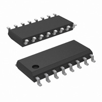
DS26LV32ATM/NOPB National Semiconductor, DS26LV32ATM/NOPB Datasheet - Page 4

DS26LV32ATM/NOPB
Manufacturer Part Number
DS26LV32ATM/NOPB
Description
IC LINE RCVR QUAD CMOS 16-SOIC
Manufacturer
National Semiconductor
Type
Receiverr
Datasheet
1.DS26LV32ATMNOPB.pdf
(10 pages)
Specifications of DS26LV32ATM/NOPB
Number Of Drivers/receivers
0/4
Protocol
RS422
Voltage - Supply
3 V ~ 3.6 V
Mounting Type
Surface Mount
Package / Case
16-SOIC (3.9mm Width)
Lead Free Status / RoHS Status
Lead free / RoHS Compliant
Other names
*DS26LV32ATM
*DS26LV32ATM/NOPB
DS26LV32ATM
*DS26LV32ATM/NOPB
DS26LV32ATM
www.national.com
t
t
t
t
t
t
t
t
Switching Characteristics - Military
PHL
PLH
PHZ
PLZ
PZH
PZL
SK1
SK2
Note 1: “Absolute Maximum ratings” are those values beyond which the safety of the device cannot be guaranteed. They are not meant to imply that the devices
should be operated at these limits. The table of “Electrical Characteristics” specifies conditions of device operation.
Note 2: Current into device pins is defined as positive. Current out of device pins is defined as negative. All voltages are referenced to ground except V
Note 3: All typicals are given for: V
Note 4: Short one output at a time to ground. Do not exceed package.
Note 5: t
Note 6: t
Note 7: t
characterization.
Note 8: All channels switching, Output Duty Cycle criteria is 40%/60% measured at 50%. Input = 1V to 2V, 50% Duty Cycle, t
by design and characterization.
Note 9: This parameter does not meet the TIA/EIA-422-B specification.
Parameter Measurement Information
±
Over Supply Voltage and -55˚C to +125˚C Operating Temperature range, unless otherwise specified.
0.1V of one another,and a Delta T
Symbol
SK1
SK2
SK3
is the |t
is the maximum skew between any two channels within a device, either edge.
is the difference in propagation delay times between any channels of any devices. This specification (maximum limit) applies to devices within V
Propagation Delay
High to Low
Propagation Delay
Low to High
Disable Time
Disable Time
Enable Time
Enable Time
Skew, |t
Skew, Pin to Pin (Note 6)
PHL
FIGURE 1. Receiver Propagation Delay and Transition Time Test Circuit (Notes 10, 11)
– t
PLH
PHL
| of a channel.
Parameter
CC
− t
A
= +3.3V, T
PLH
=
| (Note 5)
±
5˚C (between devices) within the operating temperature range. This parameter is guaranteed by design and
A
= +25˚C.
C
1, 2 )
C
3, 4 )
C
L
L
L
= 50 pF, V
= 50 pF, V
= 50 pF, V
(Notes 10, 11)
Conditions
4
CM
CM
CM
= 1.5V ( Figures
= 1.5V ( Figures
= 1.5V
Min
6
6
01290802
r
/t
f
5 ns. This parameter is guaranteed
Max
45
45
50
50
50
50
6
6
Units
ID
ns
ns
ns
ns
ns
ns
ns
ns
.
CC


