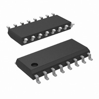
DS34C87TM/NOPB National Semiconductor, DS34C87TM/NOPB Datasheet - Page 3

DS34C87TM/NOPB
Manufacturer Part Number
DS34C87TM/NOPB
Description
IC LINE DRIVER QUAD CMOS 16-SOIC
Manufacturer
National Semiconductor
Type
Driverr
Datasheet
1.DS34C87TMNOPB.pdf
(8 pages)
Specifications of DS34C87TM/NOPB
Number Of Drivers/receivers
4/0
Protocol
RS422
Voltage - Supply
4.5 V ~ 5.5 V
Mounting Type
Surface Mount
Package / Case
16-SOIC (3.9mm Width)
Lead Free Status / RoHS Status
Lead free / RoHS Compliant
Other names
*DS34C87TM
*DS34C87TM/NOPB
DS34C87TM
*DS34C87TM/NOPB
DS34C87TM
Available stocks
Company
Part Number
Manufacturer
Quantity
Price
Company:
Part Number:
DS34C87TM/NOPB
Manufacturer:
TI
Quantity:
88
Part Number:
DS34C87TM/NOPB
Manufacturer:
NS
Quantity:
20 000
t
Skew
t
t
t
t
t
C
C
t
Skew
t
t
t
t
t
PLH
TLH
PZH
PZL
PHZ
PLZ
PLH
THL
PHZ
PLZ
PZH
PZL
DC Electrical Characteristics
Note 6: Measured per input. All other inputs at V
Note 7: This is the current sourced when a high output is shorted to ground. Only one output at a time should be shorted.
Switching Characteristics
V
PD
IN
Note 8: Skew is defined as the difference in propagation delays between complementary outputs at the 50% point.
Note 9: Output disable time is the delay from the control input being switched to the output transistors turning off. The actual disable times are less than indicated
due to the delay added by the RC time constant of the load.
Note 10: C
Comparison Table of Switching Characteristics into “LS-Type” Load
V
Note 11: This table is provided for comparison purposes only. The values in this table for the DS34C87 reflect the performance of the device but are not tested or
guaranteed.
Note 12: ESD Rating: HBM (1.5 k , 100 pF)
+ I
CC
CC
Symbol
CC
, t
, t
, t
, t
Symbol
.
THL
TLH
PHL
PHL
= 5V
= 5V, T
PD
±
determines the no load dynamic power consumption, P
10%, t
A
= +25˚C, t
Propagation Delay
Input to Output
(Note 8)
Differential Output Rise
and Fall Times
Output Disable Time
(Note 9)
Output Disable Time
(Note 9)
Output Enable Time
Output Enable Time
Propagation Delay
Input to Output
(Note 8)
Differential Output Rise
And Fall Times
Output Enable Time
Output Enable Time
Output Disable Time (Note 9)
Output Disable Time (Note 9)
Power Dissipation
Capacitance (Note 10)
Input Capacitance
r
, t
f
r
6 ns ( Figures 1, 2, 3, 4 )
Parameter
6 ns, t
Parameter
f
6 ns ( Figures 4, 5, 6, 7, 8, 9 )
CC
Inputs
or GND.
(Note 4)
1500V
(Note 4) (Continued)
C
S1 Closed, S2 Closed
C
S1 Closed, S2 Closed
C
S1 Open, S2 Closed
C
S1 Closed, S2 Open
L
L
L
L
= 50 pF, R
= 50 pF, R
= 50 pF, R
= 50 pF, R
D
Outputs
= C
Conditions
S1 Open
S1 Open
S1 Open
S1 Closed
S1 Closed
S1 Closed
S1 Closed
PD
Conditions
V
3
2
L
L
L
L
1000V
CC f + I
= 200 ,
= 200 ,
=
= 200 ,
,
CC
EIAJ (0 , 200 pF)
V
CC
, and the no load dynamic current consumption, I
Typ
1.5
Min
11
14
6
4
8
7
DS34C87
All Pins
Max
2.0
10
11
10
19
21
7
Typ
100
0.5
12
13
6
6
4
6
6
350V
Typ
10
10
17
15
11
15
DS3487
Max
11
10
25
26
12
3
8
Max
15
15
25
25
25
25
(Note 11)
S
www.national.com
= C
Units
PD
Units
pF
pF
ns
ns
ns
ns
ns
ns
ns
ns
ns
ns
ns
ns
ns
ns
V
CC
f


