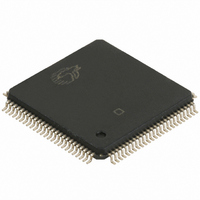
CY7C924ADX-AXI Cypress Semiconductor Corp, CY7C924ADX-AXI Datasheet - Page 25

CY7C924ADX-AXI
Manufacturer Part Number
CY7C924ADX-AXI
Description
IC TXRX HOTLINK 100LQFP
Manufacturer
Cypress Semiconductor Corp
Series
HOTlink™r
Type
Transceiverr
Datasheet
1.CY7C924ADX-AXC.pdf
(58 pages)
Specifications of CY7C924ADX-AXI
Package / Case
100-LQFP
Protocol
Fibre Channel
Voltage - Supply
4.5 V ~ 5.5 V
Mounting Type
Surface Mount
Product
Framer
Number Of Transceivers
1
Data Rate
622 Mbps
Supply Voltage (max)
5.5 V
Supply Voltage (min)
4.5 V
Supply Current (max)
250 mA
Maximum Operating Temperature
+ 85 C
Minimum Operating Temperature
- 40 C
Mounting Style
SMD/SMT
Operating Supply Voltage (typ)
5V
Screening Level
Industrial
Pin Count
100
Mounting
Surface Mount
Package Type
TQFP
Operating Supply Voltage (min)
4.5V
Operating Supply Voltage (max)
5.5V
Operating Temperature (min)
-40C
Operating Temperature (max)
85C
Lead Free Status / RoHS Status
Lead free / RoHS Compliant
Number Of Drivers/receivers
-
Lead Free Status / Rohs Status
Compliant
Available stocks
Company
Part Number
Manufacturer
Quantity
Price
Company:
Part Number:
CY7C924ADX-AXI
Manufacturer:
Cypress Semiconductor Corp
Quantity:
10 000
Document #: 38-02008 Rev. *E
Table 8. Receive Output Bus Signal Map
When a serial address is received and a match is detected, the
address, and all data following that address, is passed to the
Receive FIFO (except in discard policy 3 where the address is
discarded). This continues until a serial address is received
that does not match the contents of the Address Register,
whereupon writes to the Receive FIFO are inhibited.The Serial
Address Register has a power-up default state where the
multicast field set to an all ones condition (FFh or 3FFh). When
set to this value the receiver accepts all data, regardless of the
presence or content of any received serial address. This
“promiscuous” address can also be forced by the momentary
assertion of the RESET*[1:0] pair.
The Serial Address Register is only used when the receiver is
operated with the Receive FIFO enabled (FIFOBYP* is HIGH)
and in operating modes where the discard policy is not 0 (see
Table 7 on page 23
Serial Address Register Access
The Serial Address Register is accessed through the RXDATA
bus. Both reads and writes to the register require the device to
be addressed (AM* is LOW) and for RXRST* to be asserted
(LOW).
Note
3. First bit shifted in. Others follow in numerical order interpreted from an NRZ pattern.
RXDATA Bus I/O Bit
RXRVS/RXDATA[10]
RXSOC/RXDATA[11]
RXINT/RXDATA[8]
(FIFOBYP*=HIGH)
RXINT/RXDATA[8]
(FIFOBYP*=LOW)
RXDATA[0]
RXDATA[1]
RXDATA[2]
RXDATA[3]
RXDATA[4]
RXDATA[5]
RXDATA[6]
RXDATA[7]
RXDATA[9]
BYTE8/10*
ENCBYP*
RXSC/D*
for a list of discard policies).
Character Stream
(8-bit characters)
Decoded 10-bit
RXSC/D*
RXSOC
RXRVS
RXD[0]
RXD[1]
RXD[2]
RXD[3]
RXD[4]
RXD[5]
RXD[6]
RXD[7]
RXINT
(LOW)
HIGH
HIGH
Undecoded 10-bit
Character Stream
RXD[0]
RXD[1]
RXD[2]
RXD[3]
RXD[4]
RXD[5]
RXD[6]
RXD[7]
RXD[8]
RXD[8]
RXD[9]
HIGH
LOW
Receive Decoder Mode
When accessed for write or read operations, the RXRVS
signal is used as a read/write selector, and RXSC/D* is used
to select the operating mode (multicast or unicast) of the Serial
Address Register.
[3]
Figure 6. Serial Address Register Format and Access
RXDATA[9] or [7]
MSB
0
0
0
0
(10-bit characters)
Character Stream
Decoded 10-bit
0
0
0
0
Address Register Content
Byte-Packed
RXSC/D*
RXSOC
RXRVS
RXD[0]
RXD[1]
RXD[2]
RXD[3]
RXD[4]
RXD[5]
RXD[6]
RXD[7]
RXD[8]
RXD[8]
RXD[9]
0
0
1
1
HIGH
LOW
[3]
Serial Address Register
0
0
1
1
Multicast Address write
Multicast Address read
Unicast Address read
Unicast Address write
CY7C924ADX
Undecoded 12-bit
Character Stream
RXD[0]
RXD[10]
RXD[11]
RXD[1]
RXD[2]
RXD[3]
RXD[4]
RXD[5]
RXD[6]
RXD[7]
RXD[8]
RXD[8]
RXD[9]
LOW
LOW
RXDATA[0]
Page 25 of 58
[3]
LSB
[+] Feedback


