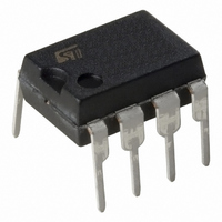
ST485BN STMicroelectronics, ST485BN Datasheet - Page 7

ST485BN
Manufacturer Part Number
ST485BN
Description
TXRX RS485/422 LOW POWER 8-DIP
Manufacturer
STMicroelectronics
Type
Transceiverr
Datasheet
1.ST485CN.pdf
(19 pages)
Specifications of ST485BN
Number Of Drivers/receivers
1/1
Protocol
RS422, RS485
Voltage - Supply
4.75 V ~ 5.25 V
Mounting Type
Through Hole
Package / Case
8-DIP (0.300", 7.62mm)
Maximum Operating Temperature
85 C
Mounting Style
Through Hole
Data Rate
2.5 Mbps
Interface
RS-422 or RS-485
Minimum Operating Temperature
- 40 C
Supply Current
+/- 2 mA
Interface Circuit Standard 1
RS-422/RS-485
Number Of Receivers
1
Number Of Transmitters
1
Number Of Transceivers
1
Data Transmission Topology
Multidrop/Multipoint
Receiver Signal Type
Differential
Transmitter Signal Type
Differential
Single Supply Voltage (typ)
5V
Single Supply Voltage (min)
4.75V
Single Supply Voltage (max)
5.25V
Dual Supply Voltage (typ)
Not RequiredV
Dual Supply Voltage (min)
Not RequiredV
Dual Supply Voltage (max)
Not RequiredV
Power Supply Requirement
Single
Operating Temp Range
-40C to 85C
Operating Temperature Classification
Industrial
Mounting
Through Hole
Pin Count
8
Package Type
PDIP
Lead Free Status / RoHS Status
Lead free / RoHS Compliant
Other names
497-6728-5
ST485BN
ST485BN
Available stocks
Company
Part Number
Manufacturer
Quantity
Price
Company:
Part Number:
ST485BN
Manufacturer:
STM
Quantity:
8 874
Part Number:
ST485BN
Manufacturer:
ST
Quantity:
20 000
Table 6.
1. All currents into device pins are positive; all cuttents out of device pins are negative; all voltages are referenced to device
2. Supply current specification is valid for loaded transmitters when V
3. Applies to peak current. See typical Operating Characteristics.
Table 7.
1. All currents into device pins are positive; all cuttents out of device pins are negative; all voltages are referenced to device
Symbol
Symbol
I
I
I
OSD1
OSD2
t
t
OSR
t
t
t
t
t
t
ground unless specified.
ground unless specified.
PLH
t
PZH
PHZ
TLH
THL
PZL
PLZ
PHL
SK
Driver short-circuit
current, V
Driver short-circuit
current, V
Receiver short-circuit
current
Propagation delay
input to output
Output skew to output
Rise or fall time
Output enable time
Output enable time
Output disable time
Output disable time
DC electrical characteristics (continued)
V
to T
Driver switching characteristics
CC
Parameter
A
Parameter
= 5 V ± 5 %, T
O
O
= 25 °C
=High
=Low
A
R
(See
R
(See
R
(See
C
(See
C
(See
C
(See
C
(See
= T
DIFF
DIFF
DIFF
L
L
L
L
V
V
V
= 100pF, S2 = Closed
= 100pF, S1 = Closed
= 15pF, S1 = Closed
= 15pF, S2 = Closed
O
O
O
MIN
Figure 4
Figure 4
Figure 4
Figure 5
Figure 5
Figure 5
Figure 5
= 54Ω, C
= 54Ω, C
= 54Ω, C
= -7 to 12V
= -7 to 12V
= 0V to V
Test conditions
Test conditions
to T
MAX
and
and
and
and
and
and
and
L1
L1
L1
CC
= C
= C
= C
(3)
(3)
, unless otherwise specified. Typical values are referred
Figure
Figure
Figure
Figure
Figure
Figure
Figure
L2
L2
L2
= 100pF
= 100pF
= 100pF
(1)
6)
6)
6)
7)
7)
7)
7)
(1)
DE
= 0V
Min.
35
35
Min.
7
10
3
-40 to 85 °C
-40 to 85 °C
Typ.
Typ. Max.
30
15
70
70
70
70
5
Value
Max.
Value
250
250
95
60
10
40
90
90
90
90
-55 to 125 °C
-55 to 125°C
Min.
Min.
35
35
7
3
Max.
Max.
250
250
95
70
10
45
90
90
90
90
Unit
Unit
mA
mA
mA
ns
ns
ns
ns
ns
ns
ns
7/19


