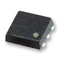
S-1711C3030-I6T1G Seiko Instruments, S-1711C3030-I6T1G Datasheet - Page 26

S-1711C3030-I6T1G
Manufacturer Part Number
S-1711C3030-I6T1G
Description
Low Dropout (LDO) Regulators DUAL Linear LDO reg Hi70uA Iq 150mA Iout
Manufacturer
Seiko Instruments
Datasheet
1.S-1711C3030-I6T1G.pdf
(44 pages)
Specifications of S-1711C3030-I6T1G
Polarity
Positive
Input Voltage Max
7 V
Output Voltage
3 V
Output Type
Fixed
Dropout Voltage (max)
3 V at 150 mA
Output Current
150 mA
Load Regulation
20 mV
Voltage Regulation Accuracy
1 %
Maximum Power Dissipation
400 mW
Maximum Operating Temperature
+ 85 C
Mounting Style
SMD/SMT
Package / Case
SNT-6A
Lead Free Status / Rohs Status
Lead free / RoHS Compliant
26
SUPER-SMALL PACKAGE 2-CIRCUIT HIGH RIPPLE-REJECTION LOW DROPOUT CMOS VOLTAGE REGULATOR
S-1711 Series
Precautions
•
•
•
•
•
•
•
•
•
•
•
Wiring patterns for the VIN, VOUT and GND pins should be designed so that the impedance is low.
mounting an output capacitor between the VOUT and VSS pins (C
between VIN and VSS pins (C
Note that the output voltage may increase when a series regulator is used at low load current (1.0 mA or less).
Note that the output voltage may increase due to driver leakage when a series regulator is used at high
temperatures.
Generally a series regulator may cause oscillation, depending on the selection of external parts. The following
conditions are recommended for this IC. However, be sure to perform sufficient evaluation under the actual usage
conditions for selection, including evaluation of temperature characteristics.
The voltage regulator may oscillate when the impedance of the power supply is high and the input capacitor is small
or an input capacitor is not connected.
If the capacitance of the IC’s output block is small, the power supply fluctuation and load fluctuation characteristics
become worse.
equipment.
When the capacitance of the IC’s output block is small, if the power supply suddenly increases sharply, a momentary
overshoot may be output. It is therefore important to sufficiently evaluate the output voltage at power application in
the actual equipment.
The application conditions for the input voltage, output voltage, and load current should not exceed the package
power dissipation.
Do not apply an electrostatic discharge to this IC that exceeds the performance ratings of the built-in electrostatic
protection circuit.
In determining the output current, attention should be paid to the output current value specified in Table 13 in the
electrical characteristics and footnote *5) of the table.
SII claims no responsibility for any disputes arising out of or in connection with any infringement by products
including this IC of patents owned by a third party.
Use input/output capacitor which has good temperature characteristics (conforming to the ceramic capacitor EIA
X5R (JIS B) characteristics).
Input capacitor (C
Output capacitor (C
Equivalent series resistance (ESR):
It is therefore important to sufficiently evaluate the output voltage fluctuation in the actual
IN
):
L1
, C
L2
IN
):
), the distance from the capacitors to these pins should be as short as possible.
Seiko Instruments Inc.
1.0 μF or more
1.0 μF or more
1.0 Ω or less
L1
, C
L2
) and a capacitor for stabilizing the input
Rev.3.0
When
_00


