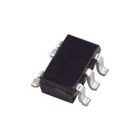
CAT6219-180TD-GT3 ON Semiconductor, CAT6219-180TD-GT3 Datasheet - Page 2

CAT6219-180TD-GT3
Manufacturer Part Number
CAT6219-180TD-GT3
Description
Low Dropout (LDO) Regulators LDO,1.8V,300mA
Manufacturer
ON Semiconductor
Datasheet
1.CAT6219-180TD-GT3.pdf
(10 pages)
Specifications of CAT6219-180TD-GT3
Number Of Outputs
1
Polarity
Positive
Input Voltage Max
5.5 V
Output Voltage
1.8 V
Output Type
Fixed
Dropout Voltage (max)
0.4 V at 500 mA
Output Current
500 mA
Line Regulation
0.2 % / V
Load Regulation
1.5 %
Voltage Regulation Accuracy
1 %
Maximum Operating Temperature
+ 125 C
Mounting Style
SMD/SMT
Package / Case
TSOT-23
Minimum Operating Temperature
- 40 C
Lead Free Status / Rohs Status
Lead free / RoHS Compliant
Available stocks
Company
Part Number
Manufacturer
Quantity
Price
Part Number:
CAT6219-180TD-GT3
Manufacturer:
ON/安森美
Quantity:
20 000
output. It has a 2.5MΩ pull-down resistor, which
assures that if EN pin is left open, the circuit is disabled.
VOUT is the LDO regulator output. A small 2.2μF
ceramic bypass capacitor is required between the
VOUT pin and ground. For better transient response,
its value can be increased to 4.7μF.
CAT6219
PIN DESCRIPTIONS
PIN FUNCTION
VIN is the supply pin for the LDO. A small 1μF
ceramic bypass capacitor is required between the V
pin and ground near the device. When using longer
connections to the power supply, C
increased without limit. The operating input voltage
range is from 2.3V to 5.5V.
EN is the enable control logic (active high) for the regulator
ABSOLUTE MAXIMUM RATINGS
RECOMMENDED OPERATING CONDITIONS
Typical application circuit with external components is shown on page 1.
Notes:
(1) Exceeding maximum rating may damage the device.
(2) The maximum allowable power dissipation at any T
(3) The device is not guaranteed to work outside its operating rating.
Doc. No. MD-10009 Rev. D
Pin # Name Function
Parameter
V
V
Junction Temperature, T
Power Dissipation, P
Storage Temperature Range, T
Lead Temperature (soldering, 5 sec.)
ESD Rating (Human Body Model)
Parameter
V
V
Junction Temperature Range, T
Package Thermal Resistance (SOT23-5), θ
IN
EN
IN
EN
1
2
3
4
4
5
allowable power dissipation will result in excessive die temperature, and the regulator will go into thermal shutdown.
, V
VOUT LDO Output Voltage.
OUT
GND
BYP
ADJ
VIN
EN
Supply voltage input.
Ground reference.
Enable input (active high); a 2.5MΩ
pull-down resistor is provided.
Optional bypass capacitor connection for
noise reduction and PSRR enhancing.
Adjustable input. Feedback pin
connected to resistor divider.
D
J
S
J
IN
value can be
(1)
JA
A
(ambient temperature) is P
Internally Limited
IN
-0.3 to V
2
-40 to +125
-65 to +150
(3)
2.3 to 5.5
0 to 6.5
0 to V
Range
Rating
The capacitor should be located near the device. For
the SOT23-5 package, a continuous 500mA output
current may turn-on the thermal protection. A 250Ω
internal shutdown switch discharges the output
capacitor in the no-load condition.
GND is the ground reference for the LDO. The pin
must be connected to the ground plane on the PCB.
BYP is the reference bypass pin. An optional 0.01μF
capacitor can be connected between BYP pin and
GND to reduce the output noise and enhance the
PSRR at high frequency.
ADJ is the adjustable input pin for the adjustable
LDO. The pin is connected to the resistor voltage
divider.
+150
235
260
3
IN
IN
+0.3
V
V
2.3V
to 5.5V
OFF ON
OUT
IN
Figure 1. Adjustable Output LDO
(2)
= 1.24V
Dmax
= (T
C
1µF
(
IN
1 +
Jmax
°C/W
Unit
Unit
mW
°C
R
R
°C
°C
°C
kV
EN
V
V
VIN
V
V
1
2
)
– T
CAT6219
Characteristics subject to change without notice
GND
A
) / θ
VOUT
ADJ
JA
. Exceeding the maximum
©
Catalyst Semiconductor, Inc.
C
2.2µF
OUT
R
R
1
2
V
OUT


