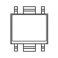
S-1172B18-E6T1G Seiko Instruments, S-1172B18-E6T1G Datasheet - Page 9

S-1172B18-E6T1G
Manufacturer Part Number
S-1172B18-E6T1G
Description
Low Dropout (LDO) Regulators Linear LDO reg Hi 70uA Iq 1000mA Iout
Manufacturer
Seiko Instruments
Datasheet
1.S-1172B18-E6T1G.pdf
(35 pages)
Specifications of S-1172B18-E6T1G
Polarity
Positive
Input Voltage Max
6 V
Output Voltage
1.8 V
Output Type
Fixed
Dropout Voltage (max)
3 V at 300 mA
Output Current
1000 mA
Load Regulation
15 mV
Voltage Regulation Accuracy
1 %
Maximum Power Dissipation
1900 mW
Maximum Operating Temperature
+ 85 C
Mounting Style
SMD/SMT
Package / Case
HSOP-6
Lead Free Status / Rohs Status
Lead free / RoHS Compliant
Available stocks
Company
Part Number
Manufacturer
Quantity
Price
Part Number:
S-1172B18-E6T1G
Manufacturer:
SEIKO/精工
Quantity:
20 000
*1.
*2.
*5.
*3.
*4.
Shutdown pin input
voltage “H”
Shutdown pin input
voltage “L”
Shutdown pin input
current “H”
Shutdown pin input
current “L”
Ripple rejection
Short-circuit current
Thermal shutdown
detection temperature
Thermal shutdown
release temperature
Rev.2.0
V
V
The output current at which the output voltage becomes 95% of V
V
V
V
voltage.
The change in temperature [mV/°C] is calculated using the following equation.
*1. Change in temperature of the output voltage
*2. Specified output voltage
*3. Output voltage temperature coefficient
The output current can be at least this value.
Due to limitation of the package power dissipation, this value may not be satisfied. Attention should be paid to the
power dissipation of the package when the output current is large.
This specification is guaranteed by design.
ΔV
OUT(S)
OUT(E)
drop
OUT3
IN1
ΔTa
OUT
Item
is the input voltage at which the output voltage becomes 98% of V
= V
is the output voltage when V
_00
[
: Specified output voltage
: Actual output voltage
mV/
IN1
The output voltage when fixing I
− (V
°
C
]
*1
*1
OUT3
=
V
× 0.98)
OUT(S)
V
V
I
I
I
T
T
HIGH RIPPLE-REJECTION LOW DROPOUT HIGH OUTPUT CURRENT CMOS VOLTAGE REGULATOR
SH
SL
SHORT
RR
Symbol
SH
SL
SD
SR
[ ]
V
*2
*2
×
ΔTa
ΔV
V
R
determined by V
output level
V
R
determined by V
output level
V
R
determined by V
output level
V
R
determined by V
output level
V
V
V
f = 1 kHz,
ΔV
I
V
f = 1 kHz,
ΔV
I
V
ON/OFF pin = ON,
V
V
ON/OFF pin = ON,
V
Junction temperature
Junction temperature
OUT
OUT
IN
IN
IN
IN
IN
IN
IN
IN
IN
OUT
IN
OUT
L
L
L
L
IN
•
rip
rip
= 1.0 kΩ,
= 1.0 kΩ,
= 1.0 kΩ,
= 1.0 kΩ,
OUT
= V
= 5.5 V,
= V
= 5.5 V,
= V
= 5.5 V,
= 5.5 V, V
= 5.5 V, V
= V
= 5.5 V,
= V
V
= 100 mA
= 100 mA
= 0 V
= 0 V
= 0.5 Vrms,
= 0.5 Vrms,
OUT
OUT(S)
OUT(S)
OUT(S)
OUT(S)
OUT(S)
OUT
[
ppm/
+ 1.0 V,
Seiko Instruments Inc.
+ 1.0 V,
+ 1.0 V,
+ 1.0 V,
(= 100 mA) and inputting V
ON/OFF
ON/OFF
+ 1.0 V or 5.5 V, and I
°
C
OUT
OUT
OUT
OUT
Conditions
Table 7 (2 / 2)
]
*3
*3
= 5.5 V
= 0 V
÷
1000
1.0 V ≤ V
4.5 V < V
1.0 V ≤ V
4.5 V < V
1.0 V ≤ V
1.2 V ≤ V
3.0 V < V
4.5 V < V
1.0 V ≤ V
4.5 V < V
OUT(S)
OUT(S)
OUT(S)
OUT(S)
OUT(S)
OUT(S)
OUT(S)
OUT(S)
OUT(S)
OUT(S)
OUT(E)
≤ 4.5 V
≤ 4.5 V
≤ 3.0 V
≤ 4.5 V
OUT
≤ 5.0 V
≤ 5.0 V
< 1.2 V
≤ 4.5 V
≤ 5.0 V
≤ 5.0 V
= 300 mA or 1000 mA.
OUT(S)
after gradually increasing the output current.
OUT3
+ 1.0 V or 5.5 V
−0.1
−0.1
Min.
(Ta = 25°C unless otherwise specified)
1.0
1.0
−
−
−
−
−
−
−
−
−
−
after gradually decreasing the input
Typ.
200
200
150
120
70
65
60
60
−
−
−
−
−
−
Max.
0.3
0.3
0.1
0.1
S-1172 Series
−
−
−
−
−
−
−
−
−
−
Unit
mA
mA
μA
μA
dB
dB
dB
dB
°C
°C
V
V
V
V
Circuit
Test
4
4
4
4
4
4
5
5
5
5
3
3
−
−
9


