AD9833BRMZ Analog Devices Inc, AD9833BRMZ Datasheet
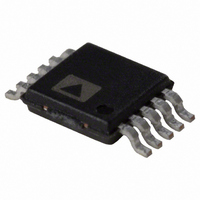
IC WAVEFORM GENERTR PROG 10-MSOP

AD9833BRMZ

Manufacturer Part Number
AD9833BRMZ
Description
IC WAVEFORM GENERTR PROG 10-MSOP
Manufacturer
Analog Devices Inc
Datasheets

Specifications of AD9833BRMZ

Resolution (bits)
10 b
Master Fclk
25MHz
Tuning Word Width (bits)
28 b
Voltage - Supply
2.3 V ~ 5.5 V
Operating Temperature
-40°C ~ 105°C
Mounting Type
Surface Mount
Package / Case
10-MSOP, Micro10™, 10-uMAX, 10-uSOP
Ic Function
Direct Digital Synthesizer
Supply Voltage Range
2.3V To 5.5V
Operating Temperature Range
-40°C To +105°C
Digital Ic Case Style
MSOP
No. Of Pins
10
Msl
MSL 3 - 168 Hours
Supplier Package
MSOP
Resolution
10 Bit
Maximum Input Frequency
25 MHz
Tuning Word Width
28 Bit
Minimum Operating Supply Voltage
2.3 V
Typical Operating Supply Voltage
2.5|3.3|5 V
Maximum Operating Supply Voltage
5.5 V
Minimum Operating Temperature
-40 °C
Maximum Operating Temperature
105 °C
Lead Free Status / RoHS Status
Lead free / RoHS Compliant
For Use With
EVAL-AD9833EBZ - BOARD EVAL FOR AD9833
Lead Free Status / Rohs Status
RoHS Compliant part Electrostatic Device

Available stocks

Company
Part Number
Manufacturer
Quantity
Price
Part Number:
AD9833BRMZ
Manufacturer:
MICRON
Quantity:
2 154
Part Number:
AD9833BRMZ
Manufacturer:
ADI
Quantity:
5 000
Part Number:
AD9833BRMZ
Manufacturer:
ADI/亚德诺
Quantity:
20 000
Part Number:
AD9833BRMZ-REEL
Manufacturer:
ADI/亚德诺
Quantity:
20 000
Part Number:
AD9833BRMZ-REEL7
Manufacturer:
AD
Quantity:
14 592
Part Number:
AD9833BRMZ-REEL7
Manufacturer:
ADI/亚德诺
Quantity:
20 000
a
REV. A
Information furnished by Analog Devices is believed to be accurate and
reliable. However, no responsibility is assumed by Analog Devices for its
use, nor for any infringements of patents or other rights of third parties that
may result from its use. No license is granted by implication or otherwise
under any patent or patent rights of Analog Devices. Trademarks and
registered trademarks are the property of their respective companies.
FEATURES
Digitally Programmable Frequency and Phase
20 mW Power Consumption at 3 V
0 MHz to 12.5 MHz Output Frequency Range
28-Bit Resolution (0.1 Hz @ 25 MHz Ref Clock)
Sinusoidal/Triangular/Square Wave Outputs
2.3 V to 5.5 V Power Supply
No External Components Required
3-Wire SPI
Extended Temperature Range: –40 C to +105 C
Power-Down Option
10-Lead MSOP Package
APPLICATIONS
Frequency Stimulus/Waveform Generation
Liquid and Gas Flow Measurement
Sensory Applications—Proximity, Motion, and Defect
Line Loss/Attenuation
Test and Medical Equipment
Sweep/Clock Generators
TDR
Detection
MCLK
®
Interface
FREQ0 REG
FREQ1 REG
AGND
FSYNC
SERIAL INTERFACE
CONTROL LOGIC
DGND
SCLK
AND
MUX
AVDD/
DVDD
SDATA
PHASE0 REG
PHASE1 REG
REGULATOR
CONTROL REGISTER
VDD
ACCUMULATOR
2.5V
FUNCTIONAL BLOCK DIAGRAM
PHASE
(28-BIT)
CAP/2.5V
MUX
Programmable Waveform Generator
12
Low Power 20 mW 2.3 V to 5.5 V
GENERAL DESCRIPTION
The AD9833 is a low power programmable waveform generator
capable of producing sine, triangular, and square wave outputs.
Waveform generation is required in various types of sensing,
actuation, and time domain reflectometry applications. The output
frequency and phase are software programmable, allowing easy
tuning. No external components are needed. The frequency regis-
ters are 28 bits; with a 25 MHz clock rate, resolution of 0.1 Hz
can be achieved. Similarly, with a 1 MHz clock rate, the AD9833
can be tuned to 0.004 Hz resolution.
The AD9833 is written to via a 3-wire serial interface. This serial
interface operates at clock rates up to 40 MHz and is compatible
with DSP and microcontroller standards. The device operates
with a power supply from 2.3 V to 5.5 V.
The AD9833 has a power-down function (SLEEP). This allows
sections of the device that are not being used to be powered down,
thus minimizing the current consumption of the part, e.g., the DAC
can be powered down when a clock output is being generated.
The AD9833 is available in a 10-lead MSOP package.
One Technology Way, P.O. Box 9106, Norwood, MA 02062-9106, U.S.A.
Tel: 781/329-4700
Fax: 781/326-8703
DIVIDE
BY 2
AD9833
ROM
SIN
MUX
REFERENCE
ON-BOARD
MUX
© 2003 Analog Devices, Inc. All rights reserved.
MSB
FULL-SCALE
10-BIT DAC
CONTROL
200
R
AD9833
www.analog.com
COMP
VOUT

Related parts for AD9833BRMZ

AD9833BRMZ Summary of contents

Page 1

FEATURES Digitally Programmable Frequency and Phase 20 mW Power Consumption MHz to 12.5 MHz Output Frequency Range 28-Bit Resolution (0 MHz Ref Clock) Sinusoidal/Triangular/Square Wave Outputs 2 5.5 V Power ...

Page 2

AD9833–SPECIFICATIONS Parameter SIGNAL DAC SPECIFICATIONS Resolution Update Rate V Max OUT V Min OUT V TC OUT DC Accuracy Integral Nonlinearity Differential Nonlinearity DDS SPECIFICATIONS Dynamic Specifications Signal-to-Noise Ratio Total Harmonic Distortion Spurious-Free Dynamic Range (SFDR) Wideband (0 to Nyquist) ...

Page 3

TIMING CHARACTERISTICS Parameter Limit MIN min t t – max ...

Page 4

AD9833 ABSOLUTE MAXIMUM RATINGS 25∞C, unless otherwise noted.) A VDD to AGND . . . . . . . . . . . . . . . . . . . . . . . . –0.3 V ...

Page 5

Pin Number Mnemonic Power Supply 2 VDD 3 CAP/2 DGND 9 AGND Analog Signal and Reference 1 COMP 10 VOUT Digital Interface and Control 5 MCLK 6 SDATA 7 SCLK 8 FSYNC REV. A PIN CONFIGURATION COMP VOUT ...

Page 6

AD9833–Typical Performance Characteristics 5 5.0 5V 4.5 3V 4.0 3.5 3 MCLK (MHz) TPC 1. Typical Current Consumption vs. MCLK Frequency –40 VDD = ...

Page 7

RWB 100 ST 100 SEC VWB 30 FREQUENCY (Hz) TPC MHz, MCLK f = 2.4 kHz, Frequency OUT Word = 000FBA9 0 –10 ...

Page 8

AD9833 TERMINOLOGY Integral Nonlinearity This is the maximum deviation of any code from a straight line passing through the endpoints of the transfer function. The end- points of the transfer function are zero scale, a point 0.5 LSB below the ...

Page 9

Numerically Controlled Oscillator Plus Phase Modulator This consists of two frequency select registers, a phase accumu- lator, two phase offset registers, and a phase offset adder. The main component of the NCO is a 28-bit phase accumulator. Continuous time signals ...

Page 10

AD9833 Control Register The AD9833 contains a 16-bit control register that sets up the AD9833 as the user wants to operate it. All control bits, except MODE, are sampled on the internal negative edge of MCLK. Table II describes the ...

Page 11

Table II. Description of Bits in the Control Register (continued) Bit Name Function D6 SLEEP12 SLEEP12 = 1 powers down the on-chip DAC. This is useful when the AD9833 is used to output the MSB of the DAC data. SLEEP12 ...

Page 12

AD9833 If the user wants to change the entire contents of a frequency regis- ter, two consecutive writes to the same address must be performed since the frequency registers are 28 bits wide. The first write will contain the 14 ...

Page 13

Sinusoidal Output The SIN ROM is used to convert the phase information from the frequency and phase registers into amplitude information that results in a sinusoidal signal at the output. To have a sinusoidal output from the VOUT pin, set ...

Page 14

AD9833 OUT YES CHANGE FSELECT? YES CHANGE FREQUENCY REGISTER? CONTROL REGISTER WRITE (SEE TABLE XI) Figure 7. Flow Chart for AD9833 Initialization and Operation DATA WRITE SEE FIGURE 9 SELECT DATA SOURCES WAIT 8/9 MCLK CYCLES DAC ...

Page 15

DATA WRITE WRITE A FULL 28-BIT WORD TO A FREQUENCY REGISTER? YES (CONTROL REGISTER WRITE) B28 (D13 WRITE TWO CONSECUTIVE 16-BIT WORDS (SEE TABLE V FOR EXAMPLE) WRITE ANOTHER FULL 28-BIT WORD TO A YES FREQUENCY REGISTER? NO ...

Page 16

AD9833 68HC11/68L11* PC7 MOSI SCK *ADDITIONAL PINS OMITTED FOR CLARITY Figure 11. 68HC11/68L11 to AD9833 Interface AD9833 to 80C51/80L51 Interface Figure 12 shows the serial interface between the AD9833 and the 80C51/80L51 microcontroller. The microcontroller is operated in mode 0 ...

Page 17

SCLK 3 SDATA 4 FSYNC 5 DVDD 0 SCLK 13 14 SDATA 15 FSYNC MCLK ...

Page 18

AD9833 OUTLINE DIMENSIONS 10-Lead Mini Small Outline Package [MSOP] (RM-10) Dimensions shown in millimeters 3.00 BSC 6 10 4.90 BSC 3.00 BSC 1 5 PIN 1 0.50 BSC 0.95 0.85 1.10 MAX 0.23 0.75 0.08 8 0.15 0.27 SEATING 0 ...

Page 19

Revision History Location 6/03—Data Sheet changed from REV REV. A. Updated ORDERING GUIDE . . . . . . . . . . . . . . . . . . . . . . . . . ...

Page 20

–20– ...

Related keywords