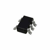
LM3460M5-1.5/NOPB National Semiconductor, LM3460M5-1.5/NOPB Datasheet - Page 6

LM3460M5-1.5/NOPB
Manufacturer Part Number
LM3460M5-1.5/NOPB
Description
IC CONTROLLER PRECISION SOT23-5
Manufacturer
National Semiconductor
Datasheet
1.LM3460M5X-1.5.pdf
(9 pages)
Specifications of LM3460M5-1.5/NOPB
Controller Type
Precision Controller
Voltage - Supply
3 V ~ 3.6 V
Current - Supply
85mA
Operating Temperature
0°C ~ 70°C
Mounting Type
Surface Mount
Package / Case
SOT-23-5, SC-74A, SOT-25
Lead Free Status / RoHS Status
Lead free / RoHS Compliant
Interface
-
Other names
LM3460M5-1.5
LM3460M5-1.5TR
LM3460M5-1.5TR
www.national.com
Setting the Output Voltage
If a regulated voltage is desired which is not available as a
standard voltage, the output voltage may be adjusted by
using an external resistive divider (see Figure 4):
FOR BEST RESULTS: SELECT R
The simplest way to calculate the resistor values is to as-
sume a value for R
R
To assure best output voltage accuracy, the value selected
for R
be used.
As the ohmic value of R
divider inside the LM3460 will cause the output voltage to
deviate from the value predicted by the formula shown.
App Circuit Technical Information
Figure 1 and Figure 2 highlight two applications of the
LM3460. This section provides details of circuit function.
1.5V/7A TYPICAL APPLICATION
Figure 1 shows the schematic of a wide-bandwidth linear
regulator which provides a regulated 1.5V output at up to 7A
of load current from a 3V-3.6V input.
The pass element of the regulator (which supplies the load
current) is made up of a three-transistor complimentary Dar-
lington composed of Q2, Q3, and Q4. The bias current
flowing through R1 will drive the pass element ON, until such
time as Q1 pulls down and takes the drive away from the
base of Q2.
The circuit regulates the output to 1.5V using the LM3460
precision controller, which sources current from its output
whenever the voltage at the IN pin reaches 1.5V.
When the LM3460 sources current from its output, it turns on
Q1 (stealing the base drive for Q2) which reduces the cur-
rent from the 1.5V regulated output. In this way, a negative
feedback loop is established which locks the output at 1.5V.
C1 and C2 are used for compensation, and should be ce-
ramic capacitors.
B
.
A
should be
FIGURE 4. Setting the Output Voltage
<
A
500Ω, and 1% tolerance resistors should
and then solve the equation shown for
A
is increased, the internal resistive
A
<
500Ω
01260310
6
C4 is required for regulator stability, and both C3 and C4
affect transient response. Circuit performance should be
carefully evaluated if substitutions are made for these two
components.
PERFORMANCE DATA
All data taken at 20˚C ambient:
LOAD/LINE REGULATION: The output voltage changed
<
voltage was varied from 3.0V-3.6V.
DROPOUT VOLTAGE: The dropout voltage (which is de-
fined as the minimum input-output voltage differential re-
quired to maintain a regulated output) was measured at 7A
and found to be 1.4V. This means that a minimum input
voltage of 2.9V is required to keep the 1.5V output in regu-
lation.
TRANSIENT RESPONSE: Transient response was tested
using a 0.2Ω power resistor connected to the output using a
mechanical contact to provide a 0-7A load current step.
When the load was applied, the change in output voltage
was seen to be
µs (see Figure 5).
HEATSINKING/COMPONENT SELECTION
HEATSINKING: As with any linear regulator, the power dis-
sipated in the pass transistor (Q4) is approximately:
Q4 must be provided with adequate heatsinking so that the
junction temperature never exceeds 150˚C.
Figure 6 shows the maximum allowable values of thermal
resistance (from heatsink-to-ambient) that must be provided
for various values of the load current.
0.1 mV as the load was increased from 0-7A, and the input
FIGURE 5. Output Transient Response
<
P = (V
5 mV with a total recovery time of about 30
IN
− V
OUT
) X I
LOAD
01260311


