DS21Q43AT+ Maxim Integrated Products, DS21Q43AT+ Datasheet
DS21Q43AT+
Specifications of DS21Q43AT+


Related parts for DS21Q43AT+


DS21Q43AT+ Summary of contents
Page 1
FEATURES § Four E1 (CEPT or PCM-30) /ISDN-PRI framing transceivers § All four framers are fully independent; transmit and receive sections of each framer are fully independent § Frames to FAS, CAS, CCS, and CRC4 formats § 8-bit parallel ...
Page 2
INTRODUCTION The DS21Q43A Quad E1 Framer is made up of five main parts: framer #0, framer #1, framer #2, framer #3, and the control port which is shared by all four framers. See the Block Diagram in Figure 1-1. ...
Page 3
DS21Q43A BLOCK DIAGRAM Figure 1-1 READER’S NOTE This data sheet assumes a particular nomenclature of the E1 operating environment. There are 32 8-bit timeslots system which are numbered 0 to 31. Timeslot 0 is transmitted first and ...
Page 4
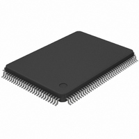
PIN-OUT CONFIGURATION Figure 1 DS21Q43A ...
Page 5
TRANSMIT PIN LIST Table 1-1 PIN SYMBOL TYPE 19 TCLK0 53 TCLK1 87 TCLK2 113 TCLK3 126 TSER0 32 TSER1 66 TSER2 92 TSER3 128 TCHCLK0 34 TCHCLK1 68 TCHCLK2 94 TCHCLK3 1 TCHBLK0 35 TCHBLK1 69 TCHBLK2 95 TCHBLK3 ...
Page 6
TFSYNC0 33 TFSYNC1 67 TFSYNC2 93 TFSYNC3 125 TSYSCLK0 31 TSYSCLK1 65 TSYSCLK2 91 TSYSCLK3 RECEIVE PIN LIST Table 1-2 PIN SYMBOL TYPE 6 RCLK0 40 RCLK1 74 RCLK2 100 RCLK3 13 RSER0 49 RSER1 83 RSER2 107 RSER3 ...
Page 7
RPOS3 I 7 RNEG0 I 41 RNEG1 I 75 RNEG2 I 101 RNEG3 I 12 RSYNC0 I/O 48 RSYNC1 I/O 82 RSYNC2 I/O 106 RSYNC3 I/O 17 RFSYNC0 O 51 RFSYNC1 O 85 RFSYNC2 O 109 RFSYNC3 O 16 ...
Page 8
CONTROL PORT/TEST/SUPPLY PIN LIST Table 1-3 PIN SYMBOL TYPE 57 TEST FS0 I 59 FS1 I 61 BTS ( (DS ...
Page 9
DS21Q43A PIN DESCRIPTION Table 1-4 Transmit Clock [TCLK]. 2.048 MHz primary clock. Used to clock data through the transmit side formatter. Necessary for proper operation of the parallel control port. Transmit Serial Data [TSER]. Transmit NRZ serial data. Sampled on ...
Page 10
Receive Channel Clock [RCHCLK]. 256 kHz clock which pulses high during the LSB of each channel. Synchronous with RCLK when the receive side elastic store is disabled. Synchronous with RSYSCLK when the receive side elastic store is enabled. Useful for ...
Page 11
Data Bus [D0 to D7] or Address/Data Bus [AD0 to AD7]. In non-multiplexed bus operation (MUX=0), serves as the data bus. In multiplexed bus operation (MUX=1), serves as an 8-bit multiplexed address/data bus. Address Bus [A0 to A5]. In non-multiplexed ...
Page 12
DS21Q43A REGISTER MAP Table 1-6 ADDRESS R BPV or Code Violation Count BPV or Code Violation Count CRC4 Count 1/FAS Error Count CRC4 Error Count E-Bit ...
Page 13
R/W Transmit Idle 4. 2A R/W Transmit Idle Definition. 2B R/W Receive Channel Blocking 1. 2C R/W Receive Channel Blocking 2. 2D R/W Receive Channel Blocking 3. 2E R/W Receive Channel Blocking 4. 2F R/W Receive Align Frame. 30 ...
Page 14
R/W Transmit Signaling 16. 50 R/W Transmit Si Bits Align Frame. 51 R/W Transmit Si Bits Non-Align Frame. 52 R/W Transmit Remote Alarm Bits. 53 R/W Transmit Sa4 Bits. 54 R/W Transmit Sa5 Bits. 55 R/W Transmit Sa6 Bits. ...
Page 15
RCR1: RECEIVE CONTROL REGISTER 1 (Address=10 Hex) (MSB) RSMF RSM RSIO SYMBOL POSITION RSMF RCR1.7 RSM RCR1.6 RSIO RCR1.5 - RCR1.4 - RCR1.3 FRC RCR1.2 SYNCE RCR1.1 RESYNC RCR1 FRC NAME AND DESCRIPTION RSYNC Multiframe Function. Only used ...
Page 16
SYNC/RESYNC CRITERIA Table 3-1 FRAME OR MULTI- FRAME LEVEL SYNC CRITERIA FAS FAS present in frame N and N+2, and FAS not present in frame CRC4 Two valid MF alignment words found within 8 ms CAS Valid ...
Page 17
TCR1: TRANSMIT CONTROL REGISTER 1 (Address=12 Hex) (MSB) ODF TFPT T16S SYMBOL POSITION ODF TCR1.7 TFPT TCR1.6 T16S TCR1.5 TUA1 TCR1.4 TSiS TCR1.3 TSA1 TCR1.2 TSM TCR1.1 TSIO TCR1.0 NOTE: 1. See Figure 11-9 for more details about how the ...
Page 18
TCR2: TRANSMIT CONTROL REGISTER 2 (Address=13 Hex) (MSB) Sa8S Sa7S Sa6S SYMBOL POSITION Sa8S TCR2.7 Sa7S TCR2.6 Sa6S TCR2.5 Sa5S TCR2.4 Sa4S TCR2.3 ODM TCR2.2 AEBE TCR2.1 PF TCR2.0 Sa5S Sa4S ODM NAME AND DESCRIPTION Sa8 Bit Select. Set to ...
Page 19
CCR1: COMMON CONTROL REGISTER 1 (Address=14 Hex) (MSB) FLB THDB3 TG802 SYMBOL POSITION FLB CCR1.7 THDB3 CCR1.6 TG802 CCR1.5 TCRC4 CCR1.4 RSM CCR1.3 RHDB3 CCR1.2 RG802 CCR1.1 RCRC4 CCR1.0 FRAMER LOOPBACK When CCR1.7 is set the DS21Q43A ...
Page 20
CCR2: COMMON CONTROL REGISTER 2 (Address=1A Hex) (MSB) ECUS VCRFS AAIS SYMBOL POSITION ECUS CCR2.7 VCRFS CCR2.6 AAIS CCR2.5 ARA CCR2.4 RSERC CCR2.3 LOTCMC CCR2.2 - CCR2.1 - CCR2.0 AUTOMATIC ALARM GENERATION When either CCR2.4 or CCR2.5 is set to ...
Page 21
CCR3: COMMON CONTROL REGISTER 3 (Address=1B Hex) (MSB) TESE TCBFS TIRFS SYMBOL POSITION TESE CCR3.7 TCBFS CCR3.6 TIRFS CCR3.5 ESR CCR3.4 - CCR3.3 - CCR3.2 TBCS CCR3.1 - CCR3.0 POWER-UP SEQUENCE On power-up, after the supplies are stable, the DS21Q43A ...
Page 22
This means that if an event occurs and a bit is set any of the registers, it will remain set until the user reads that bit. The bit will be cleared when it is read and ...
Page 23
RIR: RECEIVE INFORMATION REGISTER (Address=08 Hex) (MSB) TESF TESE LORC SYMBOL POSITION TESF RIR.7 TESE RIR.6 LORC RIR.5 RESF RIR.4 RESE RIR.3 CRCRC RIR.2 FASRC RIR.1 CASRC RIR.0 RESF RESE CRCRC NAME AND DESCRIPTION Transmit Side Elastic Store Full. Set ...
Page 24
SSR: SYNCHRONIZER STATUS REGISTER (Address=1E Hex) (MSB) CSC5 CSC4 CSC3 SYMBOL POSITION CSC5 SSR.7 CSC4 SSR.6 CSC3 SSR.5 CSC2 SSR.4 CSC0 SSR.3 FASSA SSR.2 CASSA SSR.1 CRC4SA SSR.0 CRC4 SYNC COUNTER The CRC4 Sync Counter increments each time the 8 ...
Page 25
SR1: STATUS REGISTER 1 (Address=06 Hex) (MSB) RSA1 RDMA RSA0 SYMBOL POSITION RSA1 SR1.7 RDMA SR1.6 RSA0 SR1.5 RSLIP SR1.4 RUA1 SR1.3 RRA SR1.2 RCL SR1.1 RLOS SR1.0 ALARM CRITERIA Table 4-1 ALARM SET CRITERIA RSA1 over 16 consecutive frames ...
Page 26
SR2: STATUS REGISTER 2 (Address=07 Hex) (MSB) RMF RAF TMF SYMBOL POSITION RMF SR2.7 RAF SR2.6 TMF SR2.5 SEC SR2.4 TAF SR2.3 LOTC SR2.2 RCMF SR2.1 TSLIP SR2.0 SEC TAF LOTC NAME AND DESCRIPTION Receive CAS Multiframe. Set every 2 ...
Page 27
IMR1: INTERRUPT MASK REGISTER 1 (Address=16 Hex) (MSB) RSA1 RDMA RSA0 SYMBOL POSITION RSA1 IMR1.7 RDMA IMR1.6 RSA0 IMR1.5 RSLIP IMR1.4 RUA1 IMR1.3 RRA IMR1.2 RCL IMR1.1 RLOS IMR1.0 RSLIP RUA1 RRA NAME AND DESCRIPTION Receive Signaling All 1s. 0=interrupt ...
Page 28
IMR2: INTERRUPT MASK REGISTER 2 (Address=17 Hex) (MSB) RMF RAF TMF SYMBOL POSITION RMF IMR2.7 RAF IMR2.6 TMF IMR2.5 SEC IMR2.4 TAF IMR2.3 LOTC IMR2.2 RCMF IMR2.1 TSLIP IMR2.0 5.0 ERROR COUNT REGISTERS There are a set of four counters ...
Page 29
BPV or Code Violation Counter Violation Count Register 1 (VCR1) is the most significant word and VCR2 is the least significant word of a 16-bit counter that records either BiPolar Violations (BPVs) or Code Violations (CVs). If CCR2.6=0, then ...
Page 30
E-Bit Counter E-bit Count Register 1 (EBCR1) is the most significant word and EBCR2 is the least significant word of a 10-bit counter that records Far End Block Errors (FEBE) as reported in the lines running ...
Page 31
ADDITIONAL (Sa) AND INTERNATIONAL (Si) BIT OPERATION The DS21Q43A provides for access to both the Sa and the Si bits via three different methods. The first is via a hardware scheme using the RLINK/RLCLK and TLINK/ TLCLK pins. The ...
Page 32
RAF: RECEIVE ALIGN FRAME REGISTER (Address=2F Hex) (MSB SYMBOL POSITION Si RAF.7 0 RAF.6 0 RAF.5 1 RAF.4 1 RAF.3 0 RAF.2 1 RAF.1 1 RAF.0 RNAF: RECEIVE NON-ALIGN FRAME REGISTER (Address=1F Hex) (MSB SYMBOL POSITION ...
Page 33
TAF: TRANSMIT ALIGN FRAME REGISTER (Address=20 Hex) (MSB SYMBOL POSITION Si TAF.7 0 TAF.6 0 TAF.5 1 TAF.4 1 TAF.3 0 TAF.2 1 TAF.1 1 TAF.0 TNAF: TRANSMIT NON-ALIGN FRAME REGISTER (Address=21 Hex) (MSB SYMBOL POSITION ...
Page 34
Internal Register Scheme Based on CRC4 Multiframe On the receive side, there is a set of eight registers (RSiAF, RSiNAF, RRA, RSa4 to RSa8) that report the SI and Sa bits as they are received. These registers are updated ...
Page 35
TSACR: TRANSMIT SA BIT CONTROL REGISTER (Address=1C Hex) (MSB) SiAF SiNAF RA SYMBOL POSITION SiAF TSaCR.7 SiNAF TSaCR.6 RA TSaCR.5 Sa4 TSaCR.4 Sa5 TSaCR.3 Sa6 TSaCR.2 Sa7 TSaCR.1 Sa8 TSaCR.0 Sa4 Sa5 NAME AND DESCRIPTION International Bit in Align Frame ...
Page 36
SIGNALING OPERATION The Channel Associated Signaling (CAS) bits embedded in the E1 stream can be extracted from the receive stream and inserted into the transmit stream by the DS21Q43A. Each of the 30 channels has four signaling bits (A/B/C/D) ...
Page 37
Via the SR2.7 bit, the user will be informed when the signaling registers have been loaded with data. The user has retrieve the data before it is lost. TS1 TO TS16: TRANSMIT SIGNALING REGISTERS (Address=40 ...
Page 38
The user has load the data before the old data will be retransmitted. Via the CCR3.6 bit, the user has the option to use the Transmit ...
Page 39
CLOCK BLOCKING REGISTERS The Receive Channel Blocking Register (RCBR1/ RCBR2/RCBR3/RCBR4) and the Transmit Channel Blocking Registers (TCBR1/TCBR2/TCBR3/TCBR4) control the RCHBLK and TCHBLK pins respectively. The RCHBLK and TCHCLK pins are user programmable outputs that can be forced either high ...
Page 40
TCBR1/TCBR2/TCBR3/TCBR4: DEFINITION WHEN CCR3.6=1 (MSB) CH20 CH4 CH19 CH24 CH8 CH23 CH28 CH12 CH27 CH32 CH16 CH31 *=CH1 and CH17 should be set allow the internal TS1 register to create the CAS Multiframe Alignment Word and Spare/Remote ...
Page 41
TIMING DIAGRAMS/SYNCHRONIZATION FLOWCHART/TRANSMIT DATA FLOW DIAGRAM RECEIVE SIDE TIMING Figure 11-1 NOTES: 1. RSYNC in the frame mode (RCR1.6=0). 2. RSYNC in the multiframe mode (RCR1.6=1). 3. RLCLK is programmed to output just the Sa4 bit. 4. RLINK will ...
Page 42
RECEIVE SIDE BOUNDARY TIMING (WITH ELASTIC STORE DISABLED) Figure 11-2 NOTES: 1. RCHBLK is programmed to block channel 2. 2. RLCLK is programmed to pulse during the Sa4 bits. 3. RLCLK is programmed to pulse during the SA4 and SA8 ...
Page 43
RECEIVE SIDE 1.544 MHz BOUNDARY TIMING (WITH ELASTIC STORE ENABLED) Figure 11-3 NOTES: 1. Data from the E1 channels 13, 17, 21, 25, and 29 is dropped (channel 2 from the E1 link is mapped to channel ...
Page 44
TRANSMIT SIDE TIMING Figure 11-5 NOTES: 1. TSYNC in the frame mode (TCR1.1=0). 2. TSYNC in the multiframe mode (TCR1.1=1). 3. TLINK is programmed to source only the Sa4 bit. 4. This diagram assumes both the CAS MF and the ...
Page 45
TRANSMIT SIDE BOUNDARY TIMING Figure 11-6 NOTES: 1. TSYNC is in the input mode (TCR1.0=0). 2. TSYNC is in the output mode (TCR1.0=1). 3. TCHBLK is programmed to block channel 2. 4. TLINK is programmed to source the Sa4 bits. ...
Page 46
G.802 TIMING Figure 11-7 NOTE: 1. RCHBLK or TCHBLK is programmed to pulse high during timeslots 25, and during bit 1 of timeslot 26 DS21Q43A ...
Page 47
DS21Q43A SYNCHRONIZATION FLOWCHART Figure 11 DS21Q43A ...
Page 48
DS21Q43A TRANSMIT DATA FLOW Figure 11-9 NOTE: 1. TCLK must be tied to RCLK (or RSYSCLK if the elastic store is enabled) and TSYNC must be tied to RSYNC for data to be properly sourced from RSER ...
Page 49
ABSOLUTE MAXIMUM RATINGS* Voltage on Any Pin Relative to Ground Operating Temperature Operating Temperature Storage Temperature Soldering Temperature * This is a stress rating only and functional operation of the device at these or any other conditions above those indicated ...
Page 50
INTEL BUS READ AC TIMING (BTS=0/MUX=1) Figure 12-1 INTEL BUS WRITE AC TIMING (BTS=0/MUX=1) Figure 12 DS21Q43A ...
Page 51
MOTOROLA BUS AC TIMING (BTS=1/MUX=1) Figure 12-3 AC CHARACTERISTICS - RECEIVE SIDE PARAMETER RCLK Period RCLK Pulse Width RSYSCLK Period RSYSCLK Pulse Width RSYNC Set Up to RSYSCLK Falling or RPOS/RNEG Set Up to RCLK Falling RSYNC Pulse Width RPOS/RNEG ...
Page 52
Delay RSYSCLK to RMSYNC or RSYNC Delay RCLK to RLCLK Delay RCLK to RLINK Valid See Figures 12-4 to 12-6 for details. NOTES: 1. RSYSCLK=1.544 MHz. 2. RSYSCLK=2.048 MHz. 3. RSYNC in input mode. RECEIVE SIDE AC TIMING Figure 12-4 ...
Page 53
RECEIVE SYSTEM SIDE AC TIMING Figure 12-5 NOTES: 1. RSYNC is in the output mode (RCR 1.5=0). 2. RSYNC is in the input mode (RCR1.5=1). RECEIVE LINE INTERFACE AC TIMING Figure 12 DS21Q43A ...
Page 54
AC CHARACTERISTICS - TRANSMIT SIDE PARAMETER TCLK Period TCLK Pulse Width TSYSCLK Period TSYSCLK Pulse Width TSER, TSYNC and TLINK Set Up to TCLK Falling or TSER, TFSYNC Set Up to TSYSCLK Falling TSYNC, TFSYNC Pulse Width TSER, TSYNC and ...
Page 55
AC CHARACTERISTICS - MULTIPLEXED PARALLEL PORT (MUX=1) PARAMETER Cycle Time Pulse Width, DS Low or High RD Pulse Width, DS High or Low RD Input Rise/Fall Times R/ Hold Time W R/ Setup Time Before DS High W , FS0, ...
Page 56
TRANSMIT LINE INTERFACE AC SIDE TIMING Figure 12-7 TRANSMIT SIDE AC TIMING Figure 12-8 NOTES: 1. TSYNC is in the output mode (TCR1.0=1). 2. TSYNC is in the input mode (TCR1.0=0). 3. TSER is sampled on the falling edge of ...
Page 57
TRANSMIT SYSTEM SIDE AC TIMING Figure 12-9 NOTES: 1. TSER is only sampled on the falling edge of TSYSCLK when the transmit side elastic store is enabled. 2. TCHCLK and TCHBLK are synchronous with TSYSCLK when the transmit side elastic ...
Page 58
INTEL BUS READ AC TIMING (BTS=0/MUX=0) Figure 12-10 INTEL BUS WRITE AC TIMING (BTS=0/MUX=0) Figure 12- DS21Q43A ...
Page 59
MOTOROLA BUS READ AC TIMING (BTS=1/MUX=0) Figure 12-12 MOTOROLA BUS WRITE AC TIMING (BTS=1/MUX=0) Figure 12- DS21Q43A ...
Page 60
DS21Q43A 128-PIN TQFP PKG 128-PIN DIM MIN MAX A - 1. 1.35 1.45 B 0.17 0.27 C 0.09 0.20 D 21.80 22.20 D1 20.00 BSC E 15.80 16.20 E1 14.00 BSC e 0.50 BSC L 0.45 ...